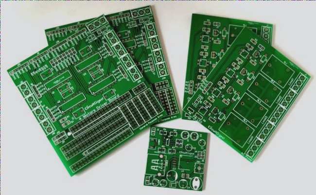
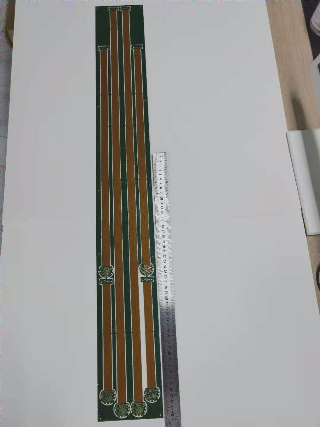
The trend in PCB design is towards lightweight and thin profiles. Alongside rigid-flex PCBs, there are intricate fields such as 3D interconnection and assembly of hybrid soft and hard boards. The hybrid board, also known as a rigid-flex board, emerged with the advent and evolution of FPCs (Flexible Printed Circuits), and is increasingly deployed across diverse applications. This board combines FPC and traditional rigid PCB characteristics through a meticulous process, forming a PCB with both flexible and rigid attributes. Such boards find utility in specialized products requiring both flexible and rigid zones.
Designing rigid-flex PCBs is significantly more intricate than conventional PCBs, necessitating careful attention, especially in the transition zones and in adhering to design rules for routing and through-holes.

1. Through-hole positioning:
During dynamic use, particularly with frequent bending of the flexible PCB, minimize the placement of vias on the soft board. These vias are susceptible to damage and cracking. Holes can be punched in reinforced areas of the soft board, but avoid the edge lines of these areas. Therefore, when designing rigid-flex PCBs, maintain a distance from the junction area during drilling, as depicted in the figure below.
2. Pad and via design:
To meet electrical requirements for pads and vias, maximize their dimensions. Use smooth transition lines to connect pads and conductors to avoid sharp angles. Independent bonding pads should include a pad toe to enhance support.
3. Routing design:
In the flex area, if lines on different layers intersect, prevent alignment where a line on the top layer directly overlays one on the bottom layer. This arrangement ensures that stresses on the upper and lower copper layers vary during board bending, reducing the risk of mechanical damage to the traces. Instead, stagger the lines and arrange paths in a crisscross pattern, as shown in the figure below.
4. Copper layout design:
For flexible reinforced PCBs, consider using a meshed or planar copper layout for better bending performance. However, for impedance control and other specific applications, assess whether a solid copper structure is necessary based on design requirements. Optimize solid copper placement in non-functional areas.
5. Distance between drilling holes and copper traces:
The “hole copper distance,” referring to the gap between a hole and adjacent copper traces, is crucial due to differences between soft and hard PCB materials. Avoid excessively tight hole copper distances, aiming for a standard spacing of 10 mils.

6. Design of Rigid-Flexible PCB Joint Area
In the rigid-flexible joint area, it is advantageous to position the FPC board to connect with the PCB board at the midpoint of the stack. Vias on the flexible portions should be treated as buried vias within the rigid-flexible joint area. Pay attention to the following in the rigid-flexible joint area:
Ensure smooth transition of traces with perpendicular alignment to the bending direction. Conductors should be uniformly distributed across the bending region. Maximize conductor width throughout the bend area. Avoid adopting PTH design for the rigid-flex transition zone.
7. Bending Radius in Rigid-Flexible PCB
The flexible bending area of a rigid-flexible PCB must withstand at least 100,000 bending cycles without open circuits, short circuits, performance degradation, or unacceptable delamination. Bending resistance should be evaluated using specialized equipment or equivalent instruments, and tested samples must meet relevant technical specifications. When designing, refer to the bending radius shown in the figure below.
Design the bending radius in relation to the thickness and number of layers of the flexible portions in the bending area. A simple guideline is R = W × T, where T is the total thickness of the flexible portion. For single-sided panels, W is 6; for double-sided panels, W is 12; and for multilayer panels, W is 24. Therefore, the minimum bending radius is 6 times the thickness for single-sided panels, 12 times for double-sided panels, and 24 times for multilayer panels, all of which shall not be less than 1.6mm.
In summary, the design of rigid-flexible PCBs is critical for integrating soft and rigid boards. When designing the flexible portion, consider different materials, thicknesses, combinations of base materials, adhesive layers, copper foils, cover layers, and reinforcement plates, as well as surface treatments and performance characteristics such as peel strength, flexural resistance, chemical properties, and operating temperatures. Special attention should be given to assembly and specific applications of the designed flex board. Design rules in this regard can refer to IPC standards: IPC-D-249 and IPC-2233.
Furthermore, for precision in processing rigid-flexible PCBs with soft plates, international standards recommend: line width of 50 μm and aperture of 0.1mm for more than 10 layers. Domestic standards suggest: line width of 75 μm and aperture of 0.2mm for 4 layers. These guidelines should be considered and referenced in specific designs.
Designing rigid-flex PCBs is significantly more intricate than conventional PCBs, necessitating careful attention, especially in the transition zones and in adhering to design rules for routing and through-holes.
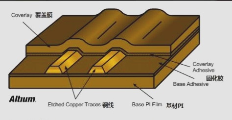
1. Through-hole positioning:
During dynamic use, particularly with frequent bending of the flexible PCB, minimize the placement of vias on the soft board. These vias are susceptible to damage and cracking. Holes can be punched in reinforced areas of the soft board, but avoid the edge lines of these areas. Therefore, when designing rigid-flex PCBs, maintain a distance from the junction area during drilling, as depicted in the figure below.
2. Pad and via design:
To meet electrical requirements for pads and vias, maximize their dimensions. Use smooth transition lines to connect pads and conductors to avoid sharp angles. Independent bonding pads should include a pad toe to enhance support.
3. Routing design:
In the flex area, if lines on different layers intersect, prevent alignment where a line on the top layer directly overlays one on the bottom layer. This arrangement ensures that stresses on the upper and lower copper layers vary during board bending, reducing the risk of mechanical damage to the traces. Instead, stagger the lines and arrange paths in a crisscross pattern, as shown in the figure below.
4. Copper layout design:
For flexible reinforced PCBs, consider using a meshed or planar copper layout for better bending performance. However, for impedance control and other specific applications, assess whether a solid copper structure is necessary based on design requirements. Optimize solid copper placement in non-functional areas.
5. Distance between drilling holes and copper traces:
The “hole copper distance,” referring to the gap between a hole and adjacent copper traces, is crucial due to differences between soft and hard PCB materials. Avoid excessively tight hole copper distances, aiming for a standard spacing of 10 mils.
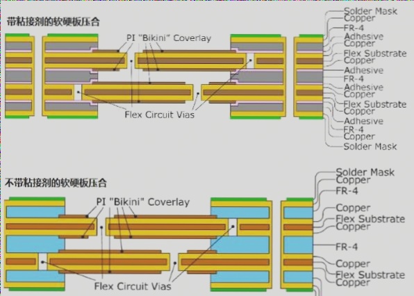
6. Design of Rigid-Flexible PCB Joint Area
In the rigid-flexible joint area, it is advantageous to position the FPC board to connect with the PCB board at the midpoint of the stack. Vias on the flexible portions should be treated as buried vias within the rigid-flexible joint area. Pay attention to the following in the rigid-flexible joint area:
Ensure smooth transition of traces with perpendicular alignment to the bending direction. Conductors should be uniformly distributed across the bending region. Maximize conductor width throughout the bend area. Avoid adopting PTH design for the rigid-flex transition zone.
7. Bending Radius in Rigid-Flexible PCB
The flexible bending area of a rigid-flexible PCB must withstand at least 100,000 bending cycles without open circuits, short circuits, performance degradation, or unacceptable delamination. Bending resistance should be evaluated using specialized equipment or equivalent instruments, and tested samples must meet relevant technical specifications. When designing, refer to the bending radius shown in the figure below.
Design the bending radius in relation to the thickness and number of layers of the flexible portions in the bending area. A simple guideline is R = W × T, where T is the total thickness of the flexible portion. For single-sided panels, W is 6; for double-sided panels, W is 12; and for multilayer panels, W is 24. Therefore, the minimum bending radius is 6 times the thickness for single-sided panels, 12 times for double-sided panels, and 24 times for multilayer panels, all of which shall not be less than 1.6mm.
In summary, the design of rigid-flexible PCBs is critical for integrating soft and rigid boards. When designing the flexible portion, consider different materials, thicknesses, combinations of base materials, adhesive layers, copper foils, cover layers, and reinforcement plates, as well as surface treatments and performance characteristics such as peel strength, flexural resistance, chemical properties, and operating temperatures. Special attention should be given to assembly and specific applications of the designed flex board. Design rules in this regard can refer to IPC standards: IPC-D-249 and IPC-2233.
Furthermore, for precision in processing rigid-flexible PCBs with soft plates, international standards recommend: line width of 50 μm and aperture of 0.1mm for more than 10 layers. Domestic standards suggest: line width of 75 μm and aperture of 0.2mm for 4 layers. These guidelines should be considered and referenced in specific designs.

