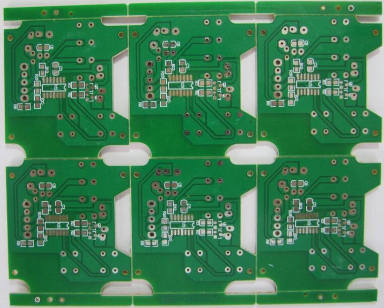
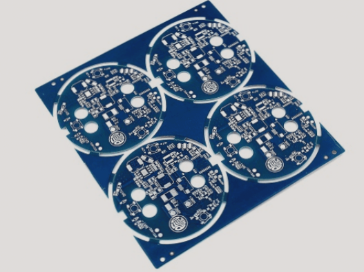
The method for addressing black sheet duplication failures in PCB boards is outlined as follows:
1. **Problem:** The width of all wires on the reproduced black and white negative film appears thin and uneven.
**Reason:**
(1) Inappropriate selection of exposure process parameters.
(2) Inferior quality of the original film.
(3) Issues with silicon control during the reworking process.
**Solution:**
(1) First, verify whether the positive or negative flip has been over-exposed, and make corrections based on the actual conditions.
(2) Assess the optical density of the original film, paying particular attention to whether the “shading density” is excessively low.
(3) Evaluate the concentration of the developer and the equipment used.
2. **Problem:** The width of the outer wire of the overturned film becomes thin or irregular.
**Reason:**
(1) The verification of PCB exposure equipment has expired.
(2) The light source is positioned too close to larger-sized film.

(3) The distance and angle of the light source reflector are not properly adjusted.
Solution:
(1) Recheck the process requirements to confirm whether the energy of the light source meets the technical specifications.
(2) Adjust the light source distance or switch to a larger exposure machine.
(3) Readjust the distance and angle of the “reflective cover.”
3. Problem: The resolution of the reproduced film is suboptimal, with blurred edges throughout.
Reason:
(1) Low quality of the original film.
(2) Ineffective vacuum system of the exposure machine.
Solution:
(1) Inspect the edge condition of the original film.
(2) A: Specifically check that the sealed connections are intact.
B: If suction is inadequate, verify if the suction hose is damaged.
4. Problem: The local resolution of the reproduced film is inadequate.
Reason:
(1) Low quality of the original film.
(2) Ineffective vacuum system of the exposure machine.
(3) Bubbles present between the negatives during exposure.
Solution:
(1) Check the leading edge condition of the original film.
(2) A: Inspect the tight joints of the vacuum system.
B: Check for any damaged sections of the air hose.
(3) Dust particles on the surface of the exposure machine require improved air extraction.
5. Problem: The optical density of the reproduced film is insufficient, particularly in the darker areas.
Reason:
(1) Incorrect development process of the reproduced film.
(2) Poor storage conditions of the original film.
(3) Deterioration of the developing device’s functionality.
Solution:
(1) Verify the development process conditions and developer concentration.
(2) Ensure storage in a room that meets process requirements, especially avoiding light exposure.
(3) Inspect and repair the developing device, focusing on temperature and time control systems.
6. Problem: Pinholes or voids appear on the graphic surface of the reproduced film.
Reason:
(1) Dust or particles on the exposure machine’s surface.
(2) Low quality of the original film.
(3) Poor quality of the original film substrate.
Solution:
(1) Thoroughly clean both the original film and the exposure table.
(2) Examine the surface condition of the original film; if needed, compare it by flipping over a second film.
(3) Conduct a trial inspection to check for pinholes or voids on the dark areas after exposure and development.
7. Problem: The circuit pattern of the reproduced film is distorted.
Reason:
(1) Incorrect temperature and humidity in the PCB working environment.
(2) Improper drying process.
(3) Inadequate pretreatment of the negative film to be reproduced.
Solution:
(1) Control the operating environment: maintain a temperature of 20-27 degrees Celsius and humidity between 40-70% RH, ideally around 55-60% RH for high-precision films.
(2) For thick films (100um), place them horizontally and blow-dry for 1-2 hours; for films of 175um, dry for 6-8 hours.
(3) Allow the film to stabilize in the film room environment for at least 24 hours.
8. Problem: The transparent area of the film is inadequate or the film base appears cloudy.
Reason:
(1) Inclusions present in the original film substrate.
(2) Poor surface quality of the original film base.
(3) Low quality of the original film.
(4) Issues in the exposure and development processes.
Solution:
(1) Select high-resolution, high-quality original film.
(2) Ensure proper temperature and humidity control in the storage environment.
(3) Test the performance and quality of the original film thoroughly.
(4) Inspect and adjust equipment conditions, including developer, fixer, and PCB production process parameters.


