PCB Boards vs. Integrated Circuits: Understanding the Differences
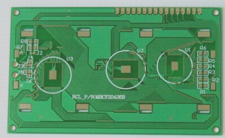
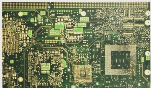
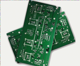
A PCB board and an integrated circuit (IC) are two essential components in electronics, but they serve different purposes. A PCB board acts as a platform for connecting various electronic components, while an IC integrates multiple electronic functions into a single chip.
Composition of a PCB Board
- Circuit and Pattern: The circuit provides electrical conduction between components, often with a grounding and power layer.
- Dielectric Layer: Ensures insulation between circuits and layers.
- Holes: Connect circuits between layers, with different types for various purposes.
- Solder Resist / Solder Mask: Protects non-soldered copper areas to prevent short circuits.
- Silkscreen: Labels components on the board for maintenance and identification.
- Surface Finish: Protects copper surfaces from oxidation for better solderability.
Key Features of PCB Boards
- High Density: Evolving alongside integrated circuit technology for increased functionality.
- High Reliability: Designed for long-term reliability through rigorous testing.
- Design Flexibility: Precision design to meet various performance requirements efficiently.
- Manufacturability: Standardized, scalable, and automated production for consistent quality.
- Testability: Comprehensive testing methods to ensure product quality and service life.
- Assemblability: Designed for standardized assembly and large-scale production.
- Maintainability: Easy repairs and replacements due to standardized design and mass production.
Advantages of Integrated Circuits
Integrated circuits offer small size, light weight, high reliability, and excellent performance, making them ideal for various applications.
Application Examples of Integrated Circuits
- 555 Touch Timer Switch: Utilizes a 555 timer IC as a monostable circuit for controlling the light based on touch input.

How to Turn on a Light with a Touch
By touching the metal plate P, a voltage signal is induced by the human body to trigger the 555 timer through C2. This changes the output at pin 3, activating the relay KS and turning on the light. Simultaneously, pin 7 disconnects internally, allowing the power supply to charge C1 via R1, starting the timing process.
When the voltage on capacitor C1 reaches 2/3 of the supply voltage, pin 7 discharges C1, switching the output at pin 3 from high to low, deactivating the relay and turning off the light, ending the timing.
The timing duration, T1, is determined by R1 and C1: T1 = 1.1 * R1 * C1. With the given component values, the timing duration is approximately 4 minutes. D1 can be either 1N4148 or 1N4001.
Single-to-Dual Power Supply Circuit in PCB Design
In this circuit, the 555 timer functions as an astable multivibrator, producing a 20 kHz square wave with a 1:1 duty cycle at pin 3. C4 charges when pin 3 is high, while C3 charges when pin 3 is low. Diodes VD1 and VD2 ensure that C3 and C4 only charge and do not discharge, with the maximum charging value equal to EC. By grounding the B terminal, a dual power supply of +/-EC is created between points A and C, with an output current exceeding 50mA.
Difference Between PCB and Integrated Circuits
An integrated circuit (IC) typically refers to a chip, like the north bridge chip on a motherboard or the internal components of a CPU, often known as an “integrated block.” On the other hand, a printed circuit board (PCB) is the physical board with printed connections for soldering components.
The IC is mounted and soldered onto the PCB, acting as its carrier. PCBs are present in nearly all electronic devices, housing components of various sizes. Apart from securing components, PCBs primarily provide electrical connections between these parts.
Simply put, an integrated circuit integrates a complete circuit into a single chip. If an IC is internally damaged, the entire chip is affected. Conversely, a PCB can be repaired by replacing individual components if they malfunction.
The above highlights the main characteristics and differences between PCB boards and integrated circuits in PCB layout design.


