The uneven copper surface area on the circuit board exacerbates the bending and warping of the board.
1. Typically, a significant area of copper foil is incorporated into the circuit board for grounding purposes, with additional large copper areas sometimes included on the Vcc layer. When these extensive copper foils are not evenly distributed on the same sheet of the circuit board during operation, it leads to uneven heat absorption and dissipation. Consequently, the circuit board will also undergo expansion and contraction. If these processes do not occur uniformly, it results in differing stress and deformation. Upon reaching the upper limit of the Tg value, the board begins to soften, leading to permanent deformation.
2. The connection points (vias) between each layer on the circuit board restrict the board’s expansion and contraction. Modern circuit boards are predominantly multi-layered, featuring rivet-like connection points (vias) between layers. These connection points can be categorized as through holes, blind holes, and buried holes. Wherever these connection points exist, they limit the board’s ability to expand and contract, indirectly contributing to bending and warping of the plate.
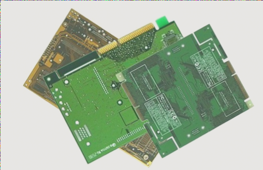
PCB circuit board impedance refers to the resistance and reactance parameters that impede alternating current. In PCB circuit board production, impedance management is crucial for several reasons:
1. The PCB circuit (the underside of the board) must accommodate the insertion of electronic components. After components are installed, it’s essential to consider their conductivity and signal transmission performance. Therefore, lower impedance is preferable, with resistivity ideally less than 1 ohm per square centimeter, preferably -6 or lower.
2. During the manufacturing process of PCB circuit boards, they go through several production steps, including copper deposition, electrolytic tin plating (or chemical plating, or thermal spray tin), and connector soldering. The materials utilized in these processes must ensure low resistivity to maintain an overall low impedance for the circuit board, thereby meeting product quality standards and ensuring normal operation.
3. Tin plating on PCB circuit boards is often the most problematic aspect of the entire production process, significantly impacting impedance. One major issue with electroless tin coatings is their susceptibility to discoloration (which can lead to oxidation or deliquescence) and poor solderability. This can result in difficult soldering, increased impedance, diminished electrical conductivity, and instability in overall board performance.
4. Signal transmission within the conductors of the PCB circuit board is diverse. When it is necessary to increase the transmission rate by raising frequency, variations in the circuit due to factors such as etching, stack thickness, and trace width can alter the impedance value. Such changes can distort signals and degrade circuit board performance, making it essential to control impedance within a specific range.
1. Typically, a significant area of copper foil is incorporated into the circuit board for grounding purposes, with additional large copper areas sometimes included on the Vcc layer. When these extensive copper foils are not evenly distributed on the same sheet of the circuit board during operation, it leads to uneven heat absorption and dissipation. Consequently, the circuit board will also undergo expansion and contraction. If these processes do not occur uniformly, it results in differing stress and deformation. Upon reaching the upper limit of the Tg value, the board begins to soften, leading to permanent deformation.
2. The connection points (vias) between each layer on the circuit board restrict the board’s expansion and contraction. Modern circuit boards are predominantly multi-layered, featuring rivet-like connection points (vias) between layers. These connection points can be categorized as through holes, blind holes, and buried holes. Wherever these connection points exist, they limit the board’s ability to expand and contract, indirectly contributing to bending and warping of the plate.

PCB circuit board impedance refers to the resistance and reactance parameters that impede alternating current. In PCB circuit board production, impedance management is crucial for several reasons:
1. The PCB circuit (the underside of the board) must accommodate the insertion of electronic components. After components are installed, it’s essential to consider their conductivity and signal transmission performance. Therefore, lower impedance is preferable, with resistivity ideally less than 1 ohm per square centimeter, preferably -6 or lower.
2. During the manufacturing process of PCB circuit boards, they go through several production steps, including copper deposition, electrolytic tin plating (or chemical plating, or thermal spray tin), and connector soldering. The materials utilized in these processes must ensure low resistivity to maintain an overall low impedance for the circuit board, thereby meeting product quality standards and ensuring normal operation.
3. Tin plating on PCB circuit boards is often the most problematic aspect of the entire production process, significantly impacting impedance. One major issue with electroless tin coatings is their susceptibility to discoloration (which can lead to oxidation or deliquescence) and poor solderability. This can result in difficult soldering, increased impedance, diminished electrical conductivity, and instability in overall board performance.
4. Signal transmission within the conductors of the PCB circuit board is diverse. When it is necessary to increase the transmission rate by raising frequency, variations in the circuit due to factors such as etching, stack thickness, and trace width can alter the impedance value. Such changes can distort signals and degrade circuit board performance, making it essential to control impedance within a specific range.

 العربية
 简体中文
简体中文 Nederlands
 English
 Français
 Deutsch
 Italiano
 日本語
日本語 한국어
한국어 Português
 Русский
 Español
 ไทย
ไทย