Benefits and Significance of Copper Paving in PCB Design
Reasons for Copper Paving:
- EMC Shielding: Ground and power supply copper areas provide shielding, with special grounds like PGND offering protection.
- PCB Process Requirements: Copper is essential for effective electroplating and to prevent deformation during lamination.
- Signal Integrity: Copper ensures a complete return path for high-frequency signals and aids in heat dissipation and device installation.
Benefits of Copper Paving:
Copper paving reduces ground wire impedance, enhancing anti-interference performance in digital circuits. While large-area grounding benefits digital circuits, analog circuits may face electromagnetic coupling interference. Mesh copper can outperform solid copper in certain scenarios.
Significance of Copper Paving:
- Reduced Loop Area: Copper laying decreases the loop area, improving performance.
- Decreased Resistance: Large copper areas reduce ground wire resistance and voltage drop, crucial for high-frequency applications.
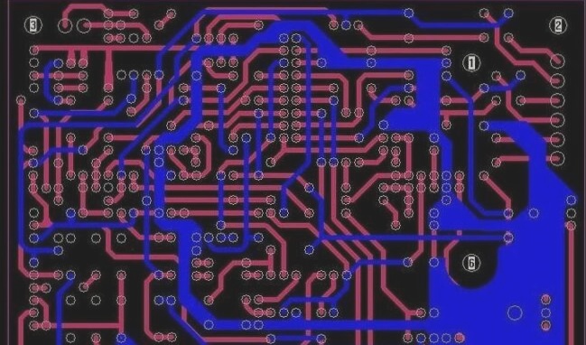
Difference Between Solid Copper and Grid Copper:
When comparing solid and grid copper, considerations include aesthetic appeal, noise suppression, and minimizing high-frequency interference on PCBs. Grid patterns help avoid sharp traces, crucial for high frequencies. Manufacturing requirements and soldering techniques influence the choice between solid and grid copper.
If you require PCB manufacturing services, feel free to contact us.