1. The IC package relies on the PCB for heat dissipation. Generally, the PCB serves as the primary cooling method for high-power semiconductor devices. A well-designed PCB heat dissipation system can have a significant impact, not only ensuring the system operates effectively but also preventing potential thermal-related failures. Proper attention to PCB layout, board structure, and component placement can significantly improve the thermal performance of medium- to high-power applications.
2. Semiconductor manufacturers often have limited control over the systems in which their devices are used. However, the design of the system that houses the IC is crucial for the overall performance of the device. For custom ICs, system designers typically collaborate closely with the manufacturer to ensure the system meets the thermal management requirements of high-power components. This early-stage cooperation helps ensure that the IC complies with both electrical and performance standards while functioning properly within the customer’s thermal environment. In contrast, many large semiconductor companies sell devices as off-the-shelf products without direct involvement with the end system. In such cases, general guidelines can be used to improve the IC’s and system’s passive cooling solutions.
3. Common semiconductor package types include exposed pad or PowerPAD™ packages. In these configurations, the chip is mounted on a metal sheet called a die pad. This die pad not only supports the chip during processing but also provides an efficient thermal path for heat dissipation. When the exposed pad is soldered to the PCB, heat is rapidly transferred from the package into the PCB, and then dissipated through the PCB layers and into the surrounding air. Exposed pad packages typically conduct about 80% of the heat through the bottom of the package into the PCB, while the remaining 20% is dissipated through the device leads and the sides of the package. Less than 1% of the heat is dissipated through the top of the package. For these exposed pad packages, an effective PCB thermal design is crucial to maintain optimal device performance.
4. The first factor that can improve thermal performance in PCB design is the layout of the components. High-power components should, whenever possible, be spaced apart to maximize the available PCB area around each component, enhancing heat conduction. Temperature-sensitive components should be isolated from high-power components to prevent thermal interference. In addition, high-power components should ideally be placed away from the PCB edges. A more centralized position on the PCB maximizes the available area for heat dissipation, helping to manage the heat more effectively. Figure 2 illustrates two identical semiconductor devices: component A and component B. Component A is positioned at the corner of the PCB, and its junction temperature is 5% higher than that of component B, which is positioned closer to the center. This is because the board area available for heat dissipation around component A is smaller, limiting its ability to cool effectively.
5. The second critical factor in PCB design is the board’s structure, which has the most significant influence on thermal performance. A general rule of thumb is that the more copper present in the PCB, the better the thermal performance of the system. The ideal thermal management scenario for semiconductor devices would involve mounting the chip on a large copper area with liquid cooling. While this is impractical for most applications, changes to the PCB structure can be made to improve heat dissipation. As the size of systems continues to shrink, it becomes more challenging to manage heat dissipation effectively. Larger PCBs allow for more surface area for heat conduction and greater flexibility in spacing high-power components, which can enhance overall thermal management.

1. Whenever possible, maximize both the number and thickness of the PCB copper ground planes. The weight of the ground plane copper is typically significant, and it serves as an excellent thermal path for dissipating heat across the entire PCB. The routing of traces on each layer also contributes to the overall copper area used for heat conduction. However, this trace routing is generally electrically and thermally isolated, which limits its effectiveness as a dedicated heat dissipation layer. The ground plane traces should be electrically connected as extensively as possible, so they can help improve heat conduction efficiency. Heat dissipation vias under the semiconductor devices assist in channeling heat into the buried layers of the PCB, allowing it to be conducted to the back of the board.
2. To enhance heat dissipation performance, the top and bottom layers of the PCB are considered “golden locations.” These areas should feature wider traces, routed away from high-power devices, to provide a thermal path for efficient heat transfer. The use of a dedicated thermal plane is an effective method for PCB heat dissipation. This thermal plane is typically positioned on the top or bottom of the PCB and is thermally connected to the device via direct copper connections or thermal vias. For inline packages (with leads on both sides), the heat conduction plane can be placed on top of the PCB in a “dog bone” shape (narrow in the center, where it aligns with the package, and wider at the ends). For four-side packages (with leads on all four sides), the thermal plane must be positioned on the back of the PCB or integrated within the PCB layers.
3. Increasing the size of the thermal plane is an effective way to improve the thermal performance of PowerPAD packages. The size of the thermal plane significantly influences thermal performance, with product datasheets typically listing these dimensions in a table format. However, it can be challenging to quantify the impact of added copper in custom PCBs. Online calculators are available where users can select a device and adjust the copper pad size to estimate its impact on heat dissipation performance in non-JEDEC PCBs. These tools demonstrate how PCB design choices directly affect thermal behavior. For four-side packages, the area of the top pad is typically just slightly smaller than the exposed pad area of the device. In this scenario, utilizing the buried or back layers is an effective method for achieving better cooling. For dual in-line packages, a “dog bone” pad style can be used to enhance heat dissipation.
4. Finally, larger PCBs can also contribute to improved cooling. When screws are used to connect the thermal plane and the ground plane for heat dissipation, certain mounting screws can also serve as effective heat paths to the system base. To balance heat conduction and cost, the number of screws should be maximized up to the point where additional screws no longer provide significant returns. Connecting the thermal plane to a metal PCB reinforcement plate increases the cooling surface area. In applications where the PCB is enclosed within a shell, controlled solder repair materials offer better thermal performance compared to air-cooled enclosures. Additionally, active cooling solutions, such as fans and heat sinks, are common methods for system cooling, though they typically require more space and may necessitate design modifications to optimize their cooling efficiency.
If your have any questions about PCB ,please contact me info@wellcircuits.com
2. Semiconductor manufacturers often have limited control over the systems in which their devices are used. However, the design of the system that houses the IC is crucial for the overall performance of the device. For custom ICs, system designers typically collaborate closely with the manufacturer to ensure the system meets the thermal management requirements of high-power components. This early-stage cooperation helps ensure that the IC complies with both electrical and performance standards while functioning properly within the customer’s thermal environment. In contrast, many large semiconductor companies sell devices as off-the-shelf products without direct involvement with the end system. In such cases, general guidelines can be used to improve the IC’s and system’s passive cooling solutions.
3. Common semiconductor package types include exposed pad or PowerPAD™ packages. In these configurations, the chip is mounted on a metal sheet called a die pad. This die pad not only supports the chip during processing but also provides an efficient thermal path for heat dissipation. When the exposed pad is soldered to the PCB, heat is rapidly transferred from the package into the PCB, and then dissipated through the PCB layers and into the surrounding air. Exposed pad packages typically conduct about 80% of the heat through the bottom of the package into the PCB, while the remaining 20% is dissipated through the device leads and the sides of the package. Less than 1% of the heat is dissipated through the top of the package. For these exposed pad packages, an effective PCB thermal design is crucial to maintain optimal device performance.
4. The first factor that can improve thermal performance in PCB design is the layout of the components. High-power components should, whenever possible, be spaced apart to maximize the available PCB area around each component, enhancing heat conduction. Temperature-sensitive components should be isolated from high-power components to prevent thermal interference. In addition, high-power components should ideally be placed away from the PCB edges. A more centralized position on the PCB maximizes the available area for heat dissipation, helping to manage the heat more effectively. Figure 2 illustrates two identical semiconductor devices: component A and component B. Component A is positioned at the corner of the PCB, and its junction temperature is 5% higher than that of component B, which is positioned closer to the center. This is because the board area available for heat dissipation around component A is smaller, limiting its ability to cool effectively.
5. The second critical factor in PCB design is the board’s structure, which has the most significant influence on thermal performance. A general rule of thumb is that the more copper present in the PCB, the better the thermal performance of the system. The ideal thermal management scenario for semiconductor devices would involve mounting the chip on a large copper area with liquid cooling. While this is impractical for most applications, changes to the PCB structure can be made to improve heat dissipation. As the size of systems continues to shrink, it becomes more challenging to manage heat dissipation effectively. Larger PCBs allow for more surface area for heat conduction and greater flexibility in spacing high-power components, which can enhance overall thermal management.
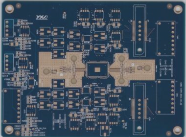
1. Whenever possible, maximize both the number and thickness of the PCB copper ground planes. The weight of the ground plane copper is typically significant, and it serves as an excellent thermal path for dissipating heat across the entire PCB. The routing of traces on each layer also contributes to the overall copper area used for heat conduction. However, this trace routing is generally electrically and thermally isolated, which limits its effectiveness as a dedicated heat dissipation layer. The ground plane traces should be electrically connected as extensively as possible, so they can help improve heat conduction efficiency. Heat dissipation vias under the semiconductor devices assist in channeling heat into the buried layers of the PCB, allowing it to be conducted to the back of the board.
2. To enhance heat dissipation performance, the top and bottom layers of the PCB are considered “golden locations.” These areas should feature wider traces, routed away from high-power devices, to provide a thermal path for efficient heat transfer. The use of a dedicated thermal plane is an effective method for PCB heat dissipation. This thermal plane is typically positioned on the top or bottom of the PCB and is thermally connected to the device via direct copper connections or thermal vias. For inline packages (with leads on both sides), the heat conduction plane can be placed on top of the PCB in a “dog bone” shape (narrow in the center, where it aligns with the package, and wider at the ends). For four-side packages (with leads on all four sides), the thermal plane must be positioned on the back of the PCB or integrated within the PCB layers.
3. Increasing the size of the thermal plane is an effective way to improve the thermal performance of PowerPAD packages. The size of the thermal plane significantly influences thermal performance, with product datasheets typically listing these dimensions in a table format. However, it can be challenging to quantify the impact of added copper in custom PCBs. Online calculators are available where users can select a device and adjust the copper pad size to estimate its impact on heat dissipation performance in non-JEDEC PCBs. These tools demonstrate how PCB design choices directly affect thermal behavior. For four-side packages, the area of the top pad is typically just slightly smaller than the exposed pad area of the device. In this scenario, utilizing the buried or back layers is an effective method for achieving better cooling. For dual in-line packages, a “dog bone” pad style can be used to enhance heat dissipation.
4. Finally, larger PCBs can also contribute to improved cooling. When screws are used to connect the thermal plane and the ground plane for heat dissipation, certain mounting screws can also serve as effective heat paths to the system base. To balance heat conduction and cost, the number of screws should be maximized up to the point where additional screws no longer provide significant returns. Connecting the thermal plane to a metal PCB reinforcement plate increases the cooling surface area. In applications where the PCB is enclosed within a shell, controlled solder repair materials offer better thermal performance compared to air-cooled enclosures. Additionally, active cooling solutions, such as fans and heat sinks, are common methods for system cooling, though they typically require more space and may necessitate design modifications to optimize their cooling efficiency.
If your have any questions about PCB ,please contact me info@wellcircuits.com

