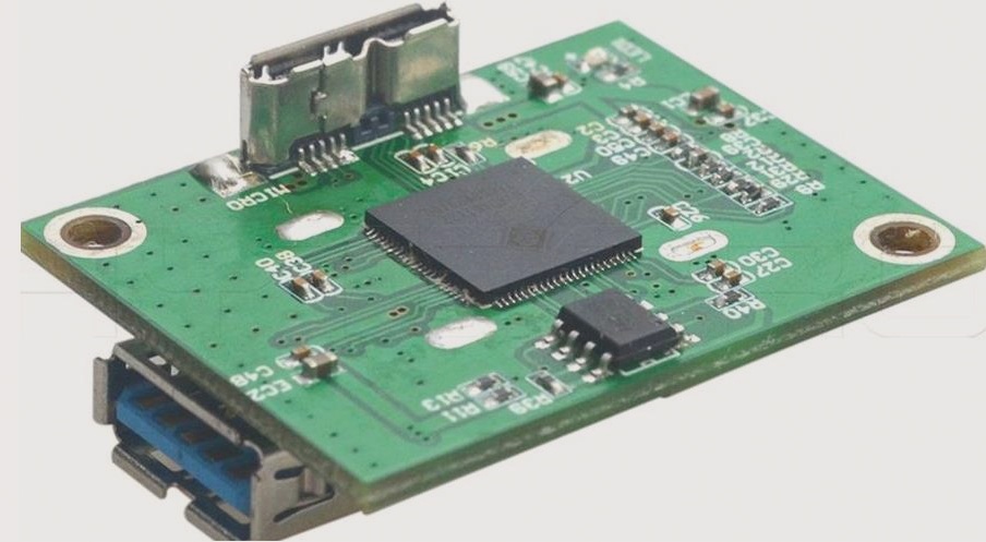
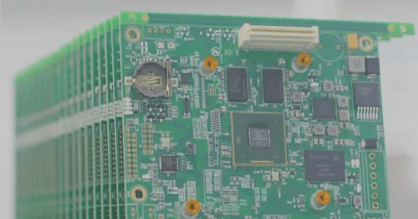
PCB Design Best Practices
Create a High-Quality Schematic Diagram
Engineers emphasize the importance of a detailed schematic diagram in PCB design. It not only helps in generating a netlist but also plays a crucial role during circuit debugging. By labeling components and noting layout concerns, the schematic becomes a valuable reference for identifying issues and collaborating with colleagues.
- Developing the habit of labeling components
- Using a hierarchical schematic for organization
- Relying on established designs
Optimize Circuit Layout
A well-thought-out PCB layout can simplify wiring tasks and enhance overall performance. Organize the layout to follow the designated signal path, separate functional modules, and prevent interference. Taking time to optimize the layout will save considerable time during wiring.

- Follow designated signal paths
- Separate functional modules
- Prevent interference
Establish Clear Guidelines
Implement wiring rules in PCB design software to minimize errors and oversights. By setting comprehensive rules, you can streamline work and utilize automatic wiring functions. Detailed rules allow tools to handle design tasks efficiently, freeing up time for other activities.
- Implement wiring rules
- Streamline work with comprehensive rules
- Utilize automatic wiring functions
Consider User Needs
Design PCBs with end users in mind, adding silkscreen information for usability and addressing production line issues for mass-produced products. Including test points and considering user needs early in the design phase can streamline future tasks and reduce support workload.
- Add silkscreen information for usability
- Address production line issues
- Include test points for improved testability
Attention to Detail is Crucial
Meticulousness is key in PCB design to avoid common mistakes such as incorrect pin assignments or device packages. Double-checking designs against actual devices and embracing simulation can help prevent errors and ensure a successful PCB design.
- Double-check designs for accuracy
- Embrace simulation for error prevention
Embrace Simulation
The Importance of Simulation in PCB Design
Many PCB design engineers may feel hesitant about utilizing simulation in their work. Some may question the value, as real-world results can differ from simulation predictions. However, relying solely on past successes is not a foolproof strategy for future projects. While simulations may not be perfect, they provide valuable insights and trends that can guide decision-making.
Although it may seem daunting at first, getting familiar with simulation parameters and gradually gaining experience is crucial. By running simulations before finalizing a PCB design, potential issues can be identified and resolved proactively, averting future problems. Embracing simulation tools will not only improve your problem-solving skills but also deepen your understanding of complex design issues.
Latest Insights in PCB Simulation
- Advanced simulation software now offers more accurate predictions than ever before.
- Real-time simulation capabilities are becoming increasingly popular in the PCB design industry.
- Cloud-based simulation platforms are revolutionizing the way engineers approach design challenges.
By incorporating simulation into your design process, you can enhance the quality and reliability of your PCB layouts, leading to more successful outcomes in your projects.