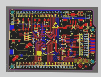
Understanding FR-4 Materials in PCB Manufacturing
The term “FR-4” commonly mentioned in the circuit board industry refers to a classification for flame-retardant materials. It represents a material grade rather than a specific material, indicating that the resin used must self-extinguish when ignited. FR-4 grade materials are commonly used in standard circuit boards, typically made from epoxy resin, fillers, and glass fiber composite materials.
Our company produces water-green and black fiberglass boards with properties such as high temperature resistance, insulation, and flame retardancy. When selecting materials for PCBs, it is crucial to consider the specific characteristics required to ensure the right products are chosen.
Flexible printed circuit boards (FPCs) are crafted using a flexible substrate through a printing process. PCB substrates can be organic or inorganic materials, with organic substrates being the most commonly used. Different PCB layers utilize various substrates, with prefabricated composite materials often used for 3- to 4-layer boards and glass-epoxy materials for double-sided boards.
Factors to Consider for SMT PCB Selection
During lead-free electronic assembly, PCBs with minimal bending, such as those made from FR-4 substrates, are essential as temperatures rise. The material’s coefficient of thermal expansion is crucial, especially for components larger than 3.2 x 1.6 mm, to prevent stress on the substrate that can affect component reliability.
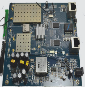
PCBs used in surface mount technology require high thermal conductivity, heat resistance, solderability, copper foil adhesion, bending strength, conductivity, low dielectric constant, and punchability. Smooth, flat surfaces free from warping, cracks, scars, and rust spots are important, along with compatibility with cleaning agents.
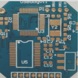
Choosing the Right PCB Thickness
The thickness of printed circuit boards ranges from 0.5mm to 6.4mm, with common sizes like 0.7mm and 1.5mm for double-sided boards with gold fingers. PCB dimensions should ideally be between 250mm x 200mm and 350mm x 250mm, with a jigsaw method recommended for smaller sizes.
Surface mount technology specifies allowable warpage for different thicknesses, with metal materials categorized into three types. As electronic plug-ins evolve towards higher pin counts and miniaturization, drilling and PCB CNC drilling equipment play essential roles in meeting interconnection demands.
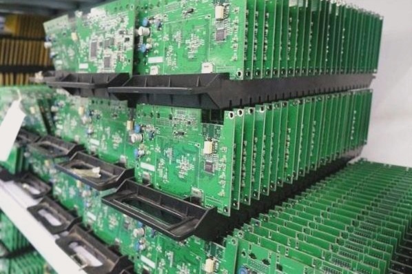
Printed Circuit Board Production Process
The production process for printed circuit boards is complex and involves a wide range of techniques, including photochemistry, electrochemistry, and thermochemistry. It consists of multiple steps, with rigid multilayer circuit boards serving as a useful example to illustrate the processing procedures.
Key Steps in PCB Production:
- Designing the Circuit Layout
- Printing the Circuit onto the Board
- Etching Away Excess Copper
- Drilling Holes for Components
- Applying Solder Mask and Silk Screen
- Testing and Quality Control
Latest Developments:
Recent advancements in PCB production techniques have focused on improving efficiency and reducing environmental impact. Innovations such as additive manufacturing and automated assembly processes are revolutionizing the industry, making PCBs more reliable and cost-effective.