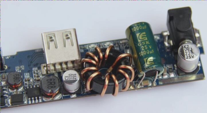
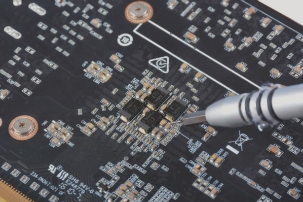
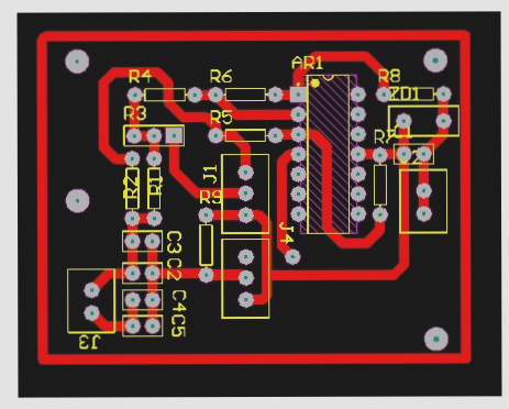
1. The typical order for placing components on a printed circuit board involves positioning them in fixed locations that closely align with the overall structure, including power sockets, indicator lights, switches, connectors, and similar elements. After placing these components, utilize the software’s LOCK function to secure them in place, preventing any accidental movement in the future.
2. Next, position special and larger components on the circuit, such as heating elements, transformers, and ICs.
3. Regarding the spacing between components and the board’s edge: ideally, all components should be situated within 3mm of the edge or at least greater than the board’s thickness. This is crucial because the assembly line for through-hole insertion and wave soldering during mass production requires a guide groove. To avoid defects at the edges caused by shaping processes, if there are numerous components on the printed circuit board and it’s necessary to exceed the 3mm limit, consider adding a 3mm auxiliary edge. This auxiliary edge should feature a V-shaped groove that can be easily broken by hand during production.

1. **Isolation between High and Low Voltage:** Many printed circuit boards (PCBs) contain both high voltage and low voltage circuits. It is crucial to keep the components of these circuits physically separated. The required isolation distance depends on the voltage level that needs to be sustained. For instance, at 2000V, a minimum distance of 2mm between the circuits is recommended, with an increase in distance proportional to the voltage. For a withstand voltage test of 3000V, the separation between high and low voltage lines should exceed 3.5mm. To prevent creepage, it is also advisable to incorporate slots between these voltage domains on the PCB.
2. **Wiring of the Printed Circuit Board:** The routing of printed wires should be as short as feasible, especially in high-frequency circuits. Wire bends should be rounded; sharp corners can adversely affect performance in high-frequency and densely wired PCBs. When connecting two panels, wires on both sides should be oriented perpendicularly, diagonally, or bent to avoid parallel alignment, which can reduce parasitic coupling. Input and output wires of the circuit should be separated as much as possible, and it’s best to insert a ground wire between these signals to mitigate feedback.
The width of the printed wire must meet electrical performance requirements while being practical for production. The minimum width is dictated by current levels but should not be less than 0.2mm. In high-density, high-precision circuits, typical wire widths and spacing can be around 0.3mm. Additionally, wire width should account for temperature rise under high current conditions. Experimental data suggests that with 50μm thick copper foil, a wire width of 1 to 1.5mm with a current of 2A results in minimal temperature rise. Thus, opting for a width of 1–1.5mm usually satisfies design criteria without significant thermal issues. Ground wires should be as thick as possible; ideally, widths of 2–3mm are recommended. This is particularly important in microprocessor circuits, where a thin ground wire can lead to variations in ground potential, destabilizing the timing signal and reducing noise margins. The 10-10 and 12-12 principles can be applied when wiring between IC pins in DIP packages: for two wires between two pins, set the pad diameter to 50mil with both line width and spacing at 10mil; for one wire, use a 64mil pad diameter with line width and spacing at 12mil.
3. **Spacing of Printed Wires:** The distance between adjacent wires must comply with electrical safety standards, and for ease of operation and manufacturing, it should be as wide as possible. The minimum spacing must accommodate withstand voltage requirements, including working voltage, additional fluctuating voltages, and peak voltages. If technical conditions permit, some metal residue between wires can reduce spacing. Designers should factor this into their voltage considerations. In low wiring density scenarios, the spacing between signal lines can be increased, and high and low-level signal lines should be kept as short as possible with increased spacing.
4. **Shielding and Grounding of Printed Wires:** The common ground wire should ideally be positioned along the edge of the PCB, maximizing the copper foil allocated to the ground wire. This arrangement enhances the shielding effect compared to a longer ground wire, improving transmission line characteristics and reducing distributed capacitance. It is best for the common ground of printed conductors to form a loop or mesh, especially in boards with numerous integrated circuits or power-consuming components, as this reduces ground potential differences and enhances noise tolerance. Additionally, the layout of ground and power supply graphics should run parallel to the data flow to bolster noise suppression capabilities. In multi-layer PCBs, several layers can serve as shielding layers, with power and ground layers typically placed on the inner layers while signal wires are routed on both inner and outer layers.
2. Next, position special and larger components on the circuit, such as heating elements, transformers, and ICs.
3. Regarding the spacing between components and the board’s edge: ideally, all components should be situated within 3mm of the edge or at least greater than the board’s thickness. This is crucial because the assembly line for through-hole insertion and wave soldering during mass production requires a guide groove. To avoid defects at the edges caused by shaping processes, if there are numerous components on the printed circuit board and it’s necessary to exceed the 3mm limit, consider adding a 3mm auxiliary edge. This auxiliary edge should feature a V-shaped groove that can be easily broken by hand during production.

1. **Isolation between High and Low Voltage:** Many printed circuit boards (PCBs) contain both high voltage and low voltage circuits. It is crucial to keep the components of these circuits physically separated. The required isolation distance depends on the voltage level that needs to be sustained. For instance, at 2000V, a minimum distance of 2mm between the circuits is recommended, with an increase in distance proportional to the voltage. For a withstand voltage test of 3000V, the separation between high and low voltage lines should exceed 3.5mm. To prevent creepage, it is also advisable to incorporate slots between these voltage domains on the PCB.
2. **Wiring of the Printed Circuit Board:** The routing of printed wires should be as short as feasible, especially in high-frequency circuits. Wire bends should be rounded; sharp corners can adversely affect performance in high-frequency and densely wired PCBs. When connecting two panels, wires on both sides should be oriented perpendicularly, diagonally, or bent to avoid parallel alignment, which can reduce parasitic coupling. Input and output wires of the circuit should be separated as much as possible, and it’s best to insert a ground wire between these signals to mitigate feedback.
The width of the printed wire must meet electrical performance requirements while being practical for production. The minimum width is dictated by current levels but should not be less than 0.2mm. In high-density, high-precision circuits, typical wire widths and spacing can be around 0.3mm. Additionally, wire width should account for temperature rise under high current conditions. Experimental data suggests that with 50μm thick copper foil, a wire width of 1 to 1.5mm with a current of 2A results in minimal temperature rise. Thus, opting for a width of 1–1.5mm usually satisfies design criteria without significant thermal issues. Ground wires should be as thick as possible; ideally, widths of 2–3mm are recommended. This is particularly important in microprocessor circuits, where a thin ground wire can lead to variations in ground potential, destabilizing the timing signal and reducing noise margins. The 10-10 and 12-12 principles can be applied when wiring between IC pins in DIP packages: for two wires between two pins, set the pad diameter to 50mil with both line width and spacing at 10mil; for one wire, use a 64mil pad diameter with line width and spacing at 12mil.
3. **Spacing of Printed Wires:** The distance between adjacent wires must comply with electrical safety standards, and for ease of operation and manufacturing, it should be as wide as possible. The minimum spacing must accommodate withstand voltage requirements, including working voltage, additional fluctuating voltages, and peak voltages. If technical conditions permit, some metal residue between wires can reduce spacing. Designers should factor this into their voltage considerations. In low wiring density scenarios, the spacing between signal lines can be increased, and high and low-level signal lines should be kept as short as possible with increased spacing.
4. **Shielding and Grounding of Printed Wires:** The common ground wire should ideally be positioned along the edge of the PCB, maximizing the copper foil allocated to the ground wire. This arrangement enhances the shielding effect compared to a longer ground wire, improving transmission line characteristics and reducing distributed capacitance. It is best for the common ground of printed conductors to form a loop or mesh, especially in boards with numerous integrated circuits or power-consuming components, as this reduces ground potential differences and enhances noise tolerance. Additionally, the layout of ground and power supply graphics should run parallel to the data flow to bolster noise suppression capabilities. In multi-layer PCBs, several layers can serve as shielding layers, with power and ground layers typically placed on the inner layers while signal wires are routed on both inner and outer layers.


