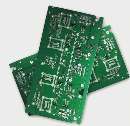
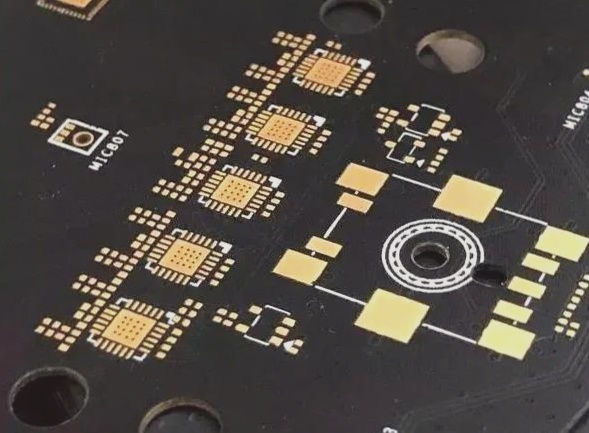
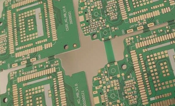
If a mechatronics engineer were to ask you what PCBs are made of, they’d most likely get a snarky reply and a laugh. But the honest answer is that it depends on what the PCB is being used for. To dive into that topic, let’s first explain what PCBs are and how they work.
There has always been a gap between the designer and whoever is manufacturing their designs in the manufacturing industry. This information gap hurts efficiency and changes what is possible in PCB design.
Since this involves a lot of science and physics, we’ll try to make it as simple as possible so engineers will understand its usefulness to them. So for those of us who understand electronics and computer science.
The artificial intelligence PCBA is used in artificial intelligence equipment, including robot motherboards, AI software and hardware, data processing boards, etc. It is mainly composed of a CPU (central processing unit) and a GPU (graphics processing unit).
After the computer completes the calculation of the program, it will return to the user as an output signal. The artificial intelligence PCBA board requires high-frequency transmission to solve the problem of data access delay, which requires more memory and a better central processing unit.

What Does The Term Artificial Intelligence Mean?
In addition to the difficulty of programming a computer to perform well in all the varied tasks of which intelligence consists, some experts question whether it is possible to formulate an adequate definition of intelligence that would allow one to decide whether a machine is truly intelligent.
AI research includes creating machines that can reason, discover meaning, generalize, or learn from past experiences. AI research also includes robotics.
Artificial Intelligence researchers and enthusiasts agree that intelligence can be defined as some combination of the following abilities:
- Learning
- Reasoning
- Problem Solving
- Perception
- Language Understanding
What Is The Relationship Between AI And PCB Design?
The advent of artificial intelligence (AI) and machine learning (ML) has provided an exciting challenge for the engineers who design printed circuit boards (PCBs). These new technologies will become increasingly challenging to keep up with the rapid amount of design changes that users request.
It is not uncommon to hear engineers talk about how they have to work hard to get things done and feel they are missing out on something important in life.
Another option that may seem less intimidating but still challenging enough would be using an open-source program such as KiCAD, which can be found on GitHub under MIT License Agreement (GPLv3 License).
Facts How Is AI Changing The Production Quality Of PCB?
With the rapid growth in demand for AI, the PCB industry will also be significantly affected. Artificial intelligence products are driving the PCB market, and AI is also changing the production quality of PCB. Here we will analyze how AI is evolving PCB production quality?
- AI Helps Manufacturers Find Problems promptly.
AI can help solve the quality issues of PCBs that were not previously possible. The production line of printed circuit boards has been automated to a certain extent, but it is challenging to ensure that 100% of products are intact without human intervention.
AI can detect potential quality issues and defects and provide them to operators on time. This type of system has been used in some industries for some time, but it is still not common in the electronics industry.
This technology can identify known defects such as missing components or soldering problems. Still, its machine learning properties can also identify new weaknesses that have not been seen before.
This system uses computer vision technology with machine learning capabilities to capture images from multiple angles and use pattern recognition algorithms to compare with other known defects, then report them to operators for further action (such as a rework or rework ).
- AI-based Optical Inspection
In PCB production, the detection of defective products relies on optical inspection, which is a vital link in improving the quality of PCB and reducing production costs.
The main problems faced by optical inspection are that it takes too long to identify defects manually, and some weaknesses are challenging to locate.
Therefore, AI-based optical inspection has been proposed, which can achieve rapid and accurate defect identification through deep learning algorithms.
- AI-assisted Soldering Machine
Soldering is another essential production process for PCBs, especially for microcontrollers and small electronic components soldered on the board. The soldering machine is used for soldering these small electronic components to the board by heating them with a nozzle at a high temperature.
If any electronic component is damaged during this process, it will cause severe problems for PCB production.
- AI-Assisted Predictive Maintenance
Predictive maintenance is an approach that uses intelligent systems, such as computers and sensors, to collect data during the operation of industrial equipment to predict when a failure may occur so that preventive measures can be taken before downtime occurs.
For example, a sensor could detect a minor malfunction in an industrial machine with predictive maintenance before the engine fails. By taking preventive measures, further damage or downtime can be avoided.
Many industries are already taking advantage of smart sensors to enable predictive maintenance. Manufacturing facilities equipped with sensors can communicate with centralized management software to alert managers about possible failures before they occur.
These systems also record data for past failures and use artificial intelligence (AI) to analyze them and determine what steps should be taken to prevent future losses.

What Does A PCB Manufacturer Require To Implement AI In Manufacturing?
AI is already in use by several companies for different applications. It’s seen that AI can be implemented in almost every manufacturing process to improve the productivity and efficiency of the process. PCB manufacturing is also one such industry that can benefit from AI integration.
AI has many applications in the PCB manufacturing industry. It can improve the quality of components, increase placement precision, pick up multiple elements at once, and much more.
But before integrating AI into the PCB manufacturing line, a manufacturer needs to understand what they need to implement.
-
- Set Your Objectives
Before you start implementing AI in your manufacturing plant, consider what you want to achieve by using this technology. Do you want to reduce costs? Do you want to increase production capacity? Do you want to improve product quality?
-
- Data and Programs
The most important thing you will need while implementing AI programs is data. You will have to collect data related to all materials used in your plant, their properties, characteristics, etc. This data will be fed into your AI program.
A complete database of all materials and equipment will ensure that your program runs smoothly and provides accurate results.
-
- Quality Control Data
Data related to quality control processes are also required for integrating AI programs into your manufacturing line.
When you try to find out why specific boards have failed, you need to know about the previous processes applied to them and what was done with them before testing them for quality control purposes. All this information should be kept in a centralized database and kept secure.
Artificial Intelligence and EDA Tools:
The real purpose of artificial intelligence, it turns out, is to make better EDA tools. Many examples of Artificial Intelligence (AI) and Electronic Design Automation (EDA) tools work together to help engineers design better products.
But AI is not just a “nice-to-have” technology – it’s becoming a requirement as integrated circuit (IC) designs become more complex and demanding.
In addition, the manufacturing process for producing ICs has reached a point where creating perfect silicon is almost impossible. As a result, yield rates are declining and have become one of the primary cost drivers in semiconductor manufacturing today.
Combining these two powerful technologies will enable engineers to find new insights in their circuit designs quickly. Here is how it works:
The first step is to collect all types of information about the circuits, such as:
- Design files – netlist, schematics, layout, DRCs, LVS, etc.
- Simulations – DC, transient, frequency response, Monte Carlo, etc.
- Layout/EM simulations – IR drop, crosstalk noise analysis (CNA), etc.
- Measurements – S-parameters, IV curves of transistors, or other device characteristics.
- Test data – parametric or functional test results or burn-in data.
The next step is “Big Data” techniques such as Hadoop or Spark cluster computing platforms can be used for swift database searches through these large volumes of data.
Bottom Line
In the past, manufacturers were always focused on making the design perfect so it could go to manufacturing. Still, with the help of AI, we can predict and avoid all these potential issues before manufacturing.
To fully realize this benefit, the design team must work with artificial intelligence at an early stage.
By incorporating AI into PCB design practices, we all feel that PCB manufacturers, component suppliers, and PCB designers will all be made better by connecting us all in ways that we could have previously imagined. Not only are we safer from errors, but better as well, and that is, after all, what it is all about.
However, suppose you’re using a CAD tool that lets you send designs over the web. In that case, it’s likely not to be an issue because of the high levels of quality control and the elimination of human interaction. Everything is done for you, leaving zero room for error or inefficiency!

