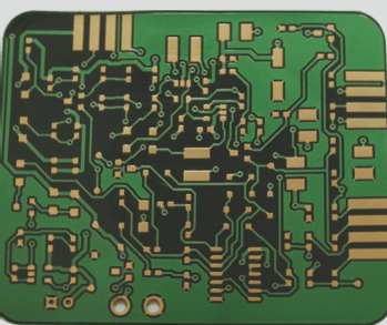
DIP (Double In-line Package) is a circuit assembly technology that involves placing through-hole components on the front of the FR-4 PCB, with the component pins passing through the PCB and being welded and assembled using wave soldering and other methods. The DIP process is essentially a plug-in welding process, and its stations can be divided into plug-in, pre-furnace inspection, repair welding, foot cutting, cleaning, post-furnace inspection, and auxiliary stations. Nordic Electronics has asked the department head of its own factory’s DIP department to discuss with you the work position and work rules of our factory, in order to improve the management of DIP work and enhance the production efficiency and quality of the DIP assembly line.

Ten Guidelines for DIP Plug-in:
1) Utilize the same manufacturing method for FR-4 PCB for consistency in manufacturing method and plug-in sequence for each PCB.
2) When there is no specific order, each station should only have one PCB at a time.
3) With the exception of the first and last stations, employees at other stations should always have a PCB on hand.
4) Typically, only one product should be completed at a time unless otherwise specified.
5) The working time for each PCB should be less than 2 minutes.
6) Install from the top left to the bottom right.
7) After completing the parts at a single position, count them with your fingers.
8) Polar parts should be classified as (up/left) and (down/right) and inserted by different personnel to prevent reverse polarity insertion.
9) First count, then insert: group small and large parts in groups of five, and insert the last part into the last position.
10) Employees must pass training before working at a station.
Solder joint peeling is a common issue in the through-hole wave soldering process, as well as in the SMT reflow soldering process. This occurs when there is a fault between the solder joint and the pad. The main reason for this phenomenon is the significant difference in thermal expansion coefficients between the lead-free alloy and the substrate, leading to excessive stress in the solder joint peeling area when fixed. Additionally, the non-eutectic property of some solder alloys contributes to this issue. To address this problem, it is important to select an appropriate solder alloy and control the cooling speed to ensure that the solder joint solidifies quickly, forming a strong binding force. Furthermore, the stress amplitude can be reduced through design, such as reducing the copper ring area of the through-hole. One popular practice in Japan is to use SMD pad design, limiting the copper ring area through green oil solder mask. However, this approach has drawbacks, including difficulty in detecting slight stripping and issues with solder joint formation between the SMD pad and green oil in terms of service life. Some suppliers may find peeling acceptable if it occurs on the wave peak through-hole solder joint, as it is not a key quality part. However, if it occurs on reflow soldering points, it should be considered a quality problem, unless the degree is very small (similar to wrinkling) in FR-4 PCB.

