PCB Layout Best Practices
- Components should be arranged on the same side of the board, except for devices like chip resistors, capacitors, and ICs which can be placed on the bottom layer if necessary.
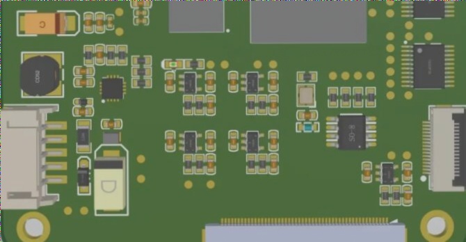
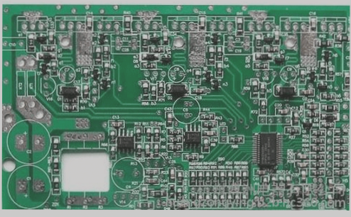
- Components should be placed on a grid, parallel or perpendicular to each other, avoiding overlap and ensuring a compact and evenly distributed layout.
- Maintain a spacing of at least 1mm between adjacent pad patterns of different components.
- Keep a distance of at least 2mm from the edge of the board, preferring a rectangular shape with an aspect ratio of 3:2 or 4:3 for boards larger than 200mm by 150mm.
PCB Design Setup Techniques
During the layout stage, use large grid points for device placement. For ICs and non-positioning connectors, utilize 50-100 mil grid points, while for smaller passive components, opt for 25 mil grid points to enhance alignment and layout aesthetics.
Effective PCB Layout Strategies
- Position functional circuit units based on the circuit flow to ensure smooth signal circulation.
- Arrange components around each unit for an integrated and compact layout, minimizing lead lengths and connections.
- For high-frequency circuits, place components in parallel to improve aesthetics and ease of installation.
Key Wiring Design Tips
- Keep trace lengths minimal to reduce lead inductance, avoiding multipoint grounding in low-frequency circuits.
- Position the common ground wire at the board edge, maximizing copper foil for enhanced shielding.
- Utilize a ground plane in double-layer boards for low-impedance ground connection.
- In multi-layer boards, design the ground layer as a mesh to prevent radiation issues from large signal loops.
- Implement a ground plane to minimize radiation loops on the PCB.


