Reasonable Component Arrangement for High-Quality PCB Layouts
Efficiently organizing components is crucial in creating a top-notch PCB board layout.
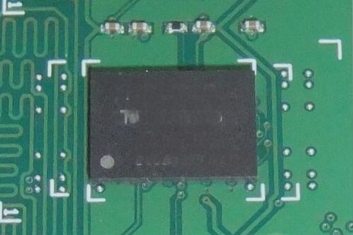
1. Component Layout
- Installation: Ensure seamless integration into the designated chassis, preventing spatial interference and short circuits.
- Mechanical Strength: Design the board to withstand external forces and vibrations, carefully placing holes for structural integrity.
- Thermal Management: Place high-power devices strategically to manage heat and minimize temperature effects on sensitive circuits.
- Signal Integrity: Address signal interference by isolating circuits and implementing proper routing and shielding measures.
- Aesthetics: Focus on neat and graceful wiring for both visual appeal and performance optimization.
2. Wiring Principles
Explore advanced anti-jamming techniques for double-sided panels:
- Wiring “Aesthetics”: Use diagonal routes instead of right angles, central organization, and proper grounding for signal integrity.
- Grounding Arrangement: Extensive ground coverage enhances system reliability, especially in weak signal processing.
- Power Line Layout and Filtering: Implement effective power line arrangements and filtering mechanisms for optimal performance.
Enhance your PCB design skills with these expert insights.

Optimizing Power Line Width for PCB Design
Many believe that using excessively thick power lines is essential, but in reality, it’s only necessary when dealing with high currents. For most applications, a power line width of around 50mil per 1A is sufficient. To ensure high-quality power supply, it is crucial to address supply fluctuations and interference by incorporating robust filter capacitors.
Strategic Capacitor Deployment
To achieve stable performance under varying frequencies and operating conditions, strategic capacitor placement is key. For digital systems, a combination of capacitors like 100uF electrolytic, 10uF tantalum, and 0.1uF surface mount capacitors around critical components can effectively manage interference.
Reducing Noise and Electromagnetic Interference
Effective noise reduction strategies play a vital role in PCB design. Utilizing appropriate speed chips, series resistors for control circuit transitions, and damping measures for relays can significantly reduce interference. Additionally, careful selection of clock frequencies, positioning of clock generators, and proper grounding of quartz crystal oscillator cases further help in mitigating electromagnetic interference.
Strategic layout considerations, such as keeping high-speed lines and clocks short and separate from noise-sensitive analog components, are crucial for maintaining overall system integrity.