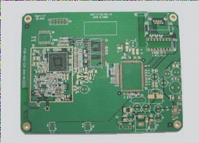
Shen’an PCB Circuit Board Production Automatic Detection Technology
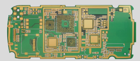
With the rise of surface mount technology, the density of circuit boards has significantly increased, making automatic inspection a crucial and cost-effective solution for manufacturing circuit boards. There are two common methods for processing and inspecting complex circuit boards: the needle bed test method and the double probe or flying probe test method.
Needle Bed Test Method
In the needle bed test method, a spring-loaded probe is connected to each inspection point on the PCB, ensuring reliable contact at each test point. These probes form a “bed of needles” controlled by specialized detection software to access information for all test points. The bed-of-needle test method can test both sides of the PCB simultaneously, but it is recommended that test points be located on the soldering surface during PCB design. The needle bed tester is costly and challenging to maintain, with probes selected based on the application.
Basic General-Purpose Grid Processor
A basic general-purpose grid processor consists of a drilled board with pin center spacings of 100, 75, or 50 mils. The pins serve as probes, establishing direct mechanical connections with electrical connectors or nodes on the circuit board. Continuity testing ensures an independent inspection of circuit board production, although the proximity of probes limits the effectiveness of the bed-of-needle testing method.
Double Probe or Flying Probe Test Method
The flying probe test method uses two or more probes mounted on a small magnetic head that can move freely on the x-y plane. Controlled by CAD or Gerber data, the probes can move independently and operate based on capacitance measurements. The tester works by pressing the PCB onto an insulating layer on a metal plate, detecting short or open circuits based on capacitance changes.
The speed of circuit board processing and testing is crucial when choosing a tester. A bed-of-needle tester can test thousands of points simultaneously, while a flying probe tester can only test a few points at a time. The mobile flying probe test method is slower but ideal for low-volume, complex circuit board production.
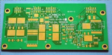
PCB Manufacturing Testing Techniques
When it comes to bare board testing in PCB manufacturing, there are various techniques and instruments available. According to Lea (1990), specialized instruments are commonly used for this purpose. However, a more cost-effective alternative is to utilize a general-purpose instrument.
Although general-purpose instruments may have a higher initial cost compared to dedicated ones, they can help reduce individual configuration expenses in the long run. For boards with pin components and surface-mounted devices, a standard grid size of 2.5 mm is typically used. In such cases, it is recommended that the test pad size should be at least 1.3 mm.
For smaller grids, such as 1 mm, the test pad size needs to be larger than 0.7 mm to ensure reliability. Using a grid smaller than 2.5 mm can make the test needle more fragile and susceptible to damage. Therefore, it is advisable to opt for a grid size larger than 2.5 mm.
Crum (1994b) proposed a solution for detecting issues in high-density PCBs by combining a universal tester (standard grid tester) with a flying probe tester. This approach can offer an accurate and cost-effective way to identify potential problems. Another method suggested by Crum is the use of a conductive rubber tester, which can pinpoint deviations from the grid.
However, it is essential to note that variations in pad height resulting from hot air leveling processes can pose challenges for establishing connections with test points.