AOI – Automatic Optical Inspection
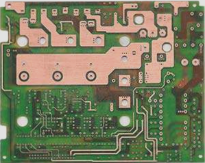
During the etching process, factors such as the etching method, etching rate, types and pH values of the etchants, or other variables directly impact the quality of the circuits. If not properly controlled, these factors can lead to defects such as short circuits, open circuits, improper circuit width, and copper residues. Therefore, post-etching boards require thorough inspection. Automatic Optical Inspection (AOI) is a widely used method that helps control scrap rates and enhance product quality.
In the AOI process, the CAM/CAD data of the PCB is commonly used as a reference for image comparison. First, the CAM/CAD data is converted into image data that can be recognized and stored by the AOI system. Various light sources are filtered through optical lenses and projected onto the PCB being inspected. The reflected light passes through different filters and reaches a receiver, which generates an electrical signal based on the light intensity.
Using its image processing card, the AOI system converts the electrical signal received by the Charge Coupled Device (CCD) camera, which scans the surface of the PCB, into a binary signal that the computer can process. This results in a binary image of the PCB. The binary image is then compared to the reference image data stored in the AOI system, which was originally converted from the CAM files. Any discrepancies or defects are identified and reported. Finally, an inspector verifies the discrepancies, completing the inspection process. Automatic Optical Inspection helps detect defects early, preventing faulty boards from progressing to the next stage, thereby reducing material waste and overall costs.
If you have any questions about PCBs and PCBA, please contact me at info@wellcircuits.com


