Advances in packaging technology resulting in finer board geometry, including the various forms of high-density interconnection (HDI), have combined with increasing data rates to exert significant pressure on the electrical test area. Fixture construction has become more expensive and necessitates enhanced process control. Advanced test methods, such as radio frequency (RF) impedance testing, are increasingly essential. Global price competition mandates cost reduction. Meanwhile, original equipment manufacturers (OEMs) demand that board manufacturers assume greater liability for defective products, thereby necessitating improved fault coverage.
This chapter is dedicated to discussing the current electrical test methods—addressing the why, what, where, when, and how—that prove effective in meeting these requirements.
Bare board test engineers are presently facing substantial changes in test requirements due to evolving product specifications. Particularly notable are changes driven by the proliferation of various HDI technologies. Common applications of HDI include direct chip attach (DCA), high-density ball grid array (BGA), and related variants often known as chip scale packaging (CSP). Additionally, there is widespread use of higher-density input/output (I/O) connectors.

Image 3: Flex bare board testing
In addition to changes in physical geometry, HDI also implies increasingly high data rates and clock speeds. Advanced methods are being applied to verify not only the product’s ability to interconnect electronic components but also to ensure signal fidelity. An analogy can be drawn comparing the impact of HDI on board technology to the effect of the sound barrier on aerodynamic flight. This analogy is directly applicable to final electrical testing.
It was once widely believed that the sound barrier was impassable, or that only Buck Rogers in his silver rocket could break through it—that beyond the speed of sound, airplanes could not operate.
As it turned out, breaking the sound barrier was challenging and required a rethinking of many aerodynamic principles. However, the resulting aircraft were still recognizable as such. They had wings, burned fuel, and met all the objectives of earlier models, but in a superior manner. Similarly, the test processes resulting from the impact of HDI on final electrical testing represent recognizable evolutions of previous methods. They employ familiar base technologies in new combinations and incorporate additional features that actually enhance test coverage rather than diminish it.

Sure, here’s the revised text:
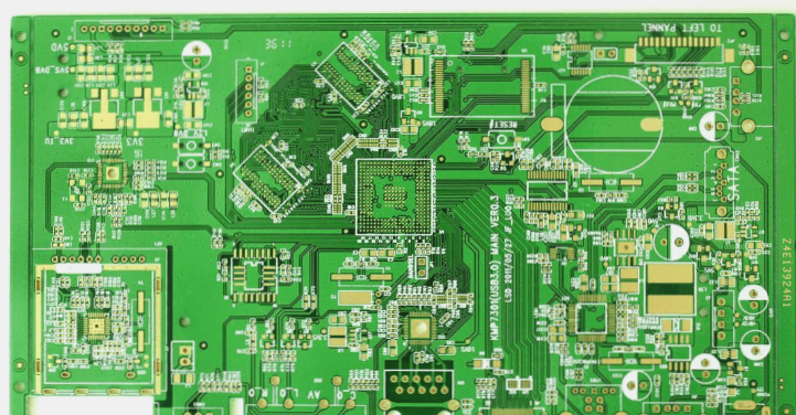
Image 2: BGA assembly on bare board
Proposals have circulated for radical new measurement approaches to electrical testing. These have included the use of electron beams, laser-stimulated photoelectric effects, and gas plasma techniques in configurations similar to existing flying probers. In each case, the board is scanned without the use of a custom test fixture. However, to date, all of these methods involve compromises in fault coverage or offer little improvement in fine-pitch performance compared to conventional methods. Most users cannot afford to relax test criteria, particularly with HDI product types which demand increased fine-pitch capability.
These finer trace and via geometries heighten the risk of latent defects, prompting increased interest in measurement methods that are most sensitive to precursor symptoms of such defects. Consequently, none of these approaches has achieved widespread adoption. Instead of witnessing radical breakthroughs, the market has experienced steady improvements in software and hardware tools. These tools effectively combine the best features of conventional test systems and cater to the growing demand for specialized test systems, especially in the small-format laminated chip carrier product type.

1: Image 3: PCB test fixture
This chapter is dedicated to discussing the current electrical test methods—addressing the why, what, where, when, and how—that prove effective in meeting these requirements.
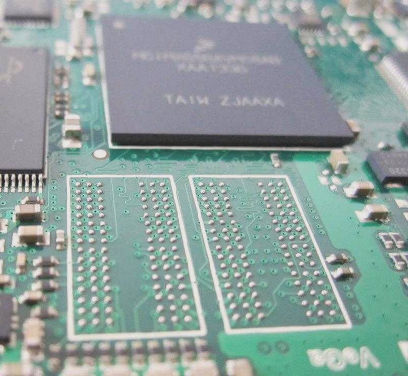
Bare board test engineers are presently facing substantial changes in test requirements due to evolving product specifications. Particularly notable are changes driven by the proliferation of various HDI technologies. Common applications of HDI include direct chip attach (DCA), high-density ball grid array (BGA), and related variants often known as chip scale packaging (CSP). Additionally, there is widespread use of higher-density input/output (I/O) connectors.
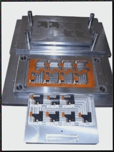
Image 3: Flex bare board testing
In addition to changes in physical geometry, HDI also implies increasingly high data rates and clock speeds. Advanced methods are being applied to verify not only the product’s ability to interconnect electronic components but also to ensure signal fidelity. An analogy can be drawn comparing the impact of HDI on board technology to the effect of the sound barrier on aerodynamic flight. This analogy is directly applicable to final electrical testing.
It was once widely believed that the sound barrier was impassable, or that only Buck Rogers in his silver rocket could break through it—that beyond the speed of sound, airplanes could not operate.
As it turned out, breaking the sound barrier was challenging and required a rethinking of many aerodynamic principles. However, the resulting aircraft were still recognizable as such. They had wings, burned fuel, and met all the objectives of earlier models, but in a superior manner. Similarly, the test processes resulting from the impact of HDI on final electrical testing represent recognizable evolutions of previous methods. They employ familiar base technologies in new combinations and incorporate additional features that actually enhance test coverage rather than diminish it.
Sure, here’s the revised text:
Image 2: BGA assembly on bare board
Proposals have circulated for radical new measurement approaches to electrical testing. These have included the use of electron beams, laser-stimulated photoelectric effects, and gas plasma techniques in configurations similar to existing flying probers. In each case, the board is scanned without the use of a custom test fixture. However, to date, all of these methods involve compromises in fault coverage or offer little improvement in fine-pitch performance compared to conventional methods. Most users cannot afford to relax test criteria, particularly with HDI product types which demand increased fine-pitch capability.
These finer trace and via geometries heighten the risk of latent defects, prompting increased interest in measurement methods that are most sensitive to precursor symptoms of such defects. Consequently, none of these approaches has achieved widespread adoption. Instead of witnessing radical breakthroughs, the market has experienced steady improvements in software and hardware tools. These tools effectively combine the best features of conventional test systems and cater to the growing demand for specialized test systems, especially in the small-format laminated chip carrier product type.
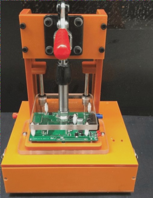
1: Image 3: PCB test fixture

