3. PCB Layout
(6) Include a decoupling capacitor (usually a monolithic capacitor with good high-frequency performance) between the power input pin of each integrated circuit and the ground. In densely populated areas on the board, it is also recommended to add a tantalum capacitor around multiple integrated circuits.
(7) Make sure to add a discharge diode (1N4148) to the relay coil.
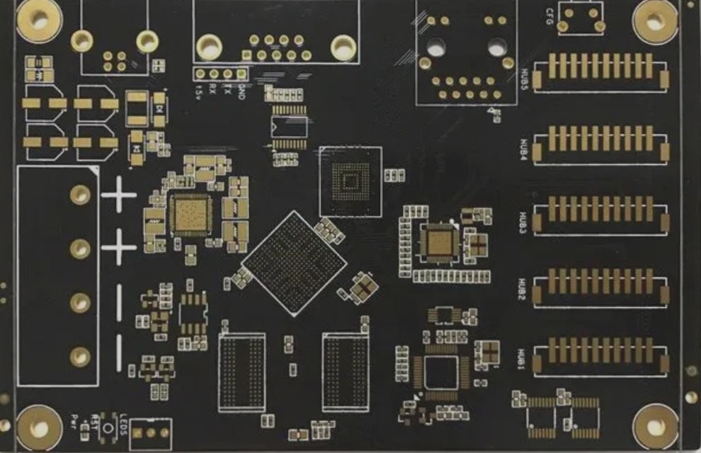
(8) When placing components, ensure a balanced, dense, and orderly layout that is not top-heavy or cluttered. Pay particular attention to the actual size (occupied area and height) of the components and the spacing between them, ensuring the electrical performance of the circuit board while also considering production and installation feasibility and convenience. Additionally, strive for neater and more aesthetically pleasing component placement by organizing identical components in the same direction, as this contributes to the overall board image and eases wiring in subsequent steps. Effort should be devoted to meticulous consideration during layout, with the possibility of preliminary wiring to address any uncertainties.
4. Wiring
The wiring process is crucial in PCB design as it directly impacts board performance. Wiring typically involves three key aspects. First, the layout must meet basic connectivity requirements to avoid scattered or floating lines, ensuring a subpar board is not produced. Second, electrical performance must be satisfied as a benchmark for PCB qualification. After layout, refine the wiring to optimize electrical performance. Finally, consider appearance – neat and orderly wiring enhances the overall appeal of the board and facilitates testing and maintenance. Even if electrical performance is good, messy wiring can detract from the board’s quality. Strive for a uniform and organized wiring layout, avoiding tangled or disordered lines while meeting all electrical requirements.


