Fourth: Classification of PCB

According to the number of circuit layers, PCB boards are classified as single-layer, double-layer, and multi-layer boards. Common multi-sided boards are generally 4-sided or 6-sided, while complex multi-sided boards can have dozens of layers.

Single-Sided Boards: These basic PCB boards have components on one side and wires on the other side (when there are SMD components on one side, the plug-in devices are on the other side). Due to the presence of wires on only one side, these PCB boards are called single-sided boards. Single-sided boards have limitations on circuit design, as the wiring cannot cross and must follow a separate path. This type of board is mostly used in older circuits.

Double-Sided Boards: These PCB boards have wiring on both sides, but a proper circuit connection between the two sides is required. The connection between such circuits is made through vias, small holes filled or coated with metal on the PCB board. Double-sided boards have twice the area of single-sided boards, solving the wiring difficulties of the single-sided boards and are more suitable for complex circuits.

Multi-Layer Boards: To increase the area for wiring, multi-layer boards incorporate multiple single or double-sided wiring boards. By using inner and outer layers in a specific configuration, printed circuit boards with four or six layers are created. These boards are known as multilayer printed circuit boards. The number of layers in the board does not necessarily correspond to the number of wiring layers, as empty layers may be added for thickness control. While most motherboards have 4 to 8 layers, technically it is possible to have up to 100 layers. Supercomputers may use highly multi-layered motherboards, but with the availability of cluster computing, the use of super-multilayered boards has declined.

Fifth: Composition of PCB

Circuit and Pattern: The circuit serves as a conductor between components, with a large copper surface designed for grounding and power distribution. The routes and drawings are created simultaneously.

Dielectric Layer: Also known as the substrate, this layer provides insulation between the circuit and other layers.

Through Hole / Via: Through holes facilitate connections between multiple levels. Larger through holes may be used for plug-in components, while non-through holes are often used for surface mounts.

Solder Resistant / Solder Mask: Not all copper surfaces require soldering, so a layer of substance (often epoxy resin) is applied to insulate non-tinned areas and prevent short circuits.

Legend / Marking / Silk Screen: These non-essential structures help identify and locate components on the board for maintenance and assembly.

Surface Finish: Various methods, such as HASL, ENIG, Immersion Silver, Immersion Tin, and OSP, are used to protect copper surfaces from oxidation and ensure proper solderability.

Sixth: Appearance of PCB

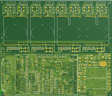
The bare board, also known as a Printed Wiring Board (PWB), is made of insulated and heat-resistant materials with copper foil conductor patterns for circuit connections. PCB boards are typically green or brown, reflecting the color of the solder mask, which protects copper wires from short circuits and excess solder. A silk screen, printed on the solder mask, helps identify component positions on the board.

Electronic components, including integrated circuits, transistors, diodes, and passive components, are mounted on the PCB. Through wire connections, electronic signals are established, enabling the functionality of the circuit.

Leave a Comment

Contact

WellCircuits
More than PCB

Upload your GerberFile(7z,rar,zip)