The ongoing advancement of economic development and the enhancement of electronic equipment production processes have provided the PCBA foundry method with an unprecedented opportunity for improvement. Today, I will discuss “the benefits of PCBA foundry materials and key production process focuses.”
1. What are the benefits of PCBA foundry materials?
Firstly, it’s well recognized that companies aiming to optimize their production need a minimum order quantity (MOQ). Due to the high costs associated with MOQ, many small and medium-sized enterprises often find themselves in a challenging position if they adopt the traditional PCB OEM model. However, with industry evolution, a smaller PCB OEM model has emerged, enabling companies to engage in OEM business even with just a few product sets. This significantly lowers the entry barriers for production and allows more electronic products to transition directly to the foundry phase after design completion, thereby greatly reducing the production cycle.

Second, in the past, engaging in PCBA OEM business required manufacturers to maintain a significant production volume. When production batches were small, manufacturers incurred substantial additional management costs. However, with the evolution of the foundry industry, small enterprises can now access foundry services. Current manufacturers no longer face these previous challenges; they only adjust costs based on the customer’s order, relieving customers of direct management expenses. This not only facilitates customer acceptance but also lowers the barriers for new businesses to enter the market.
PCBA Foundry Material
Second, the process focus of PCBA foundry production
The technological emphasis in PCBA foundry production is crucial for mastering the related processes and methodologies. Understanding the key aspects of SMT patch proofing is akin to grasping the essence of SMT technology. Regardless of how complex or variable the soldering issues encountered may be, PCBA factories can effectively analyze and resolve problems in a targeted manner.
For instance, if one does not recognize that the BGA soldering process on a PCB involves both collapse and deformation during small batch SMT proofing, it becomes challenging to comprehend the significance of peak temperature and soldering duration. Additionally, if there is a lack of awareness that the properties of lead solder paste differ from those of lead-free BGA, understanding the complexities of the mixing process becomes difficult.
Thus, grasping the key points of PCB processing while learning SMT patch processing technology is essential. This foundational knowledge is vital for analyzing and addressing complex SMT patch proofing challenges. Surface assembly soldering technology, specifically the SMT patch proofing process, is intricate and continuously evolving—from leaded to eco-friendly lead-free processes, and from large to micro-pad soldering. Despite ongoing advancements in PCB processing, the fundamental principles remain unchanged.
Mastering the essential processes of PCBA production, along with understanding the causes and solutions for common soldering issues, can enhance the maturity and stability of SMT patch technology, establishing an effective quality control system. This knowledge is practically significant for swiftly addressing SMT processing and production technology challenges.
1. What are the benefits of PCBA foundry materials?
Firstly, it’s well recognized that companies aiming to optimize their production need a minimum order quantity (MOQ). Due to the high costs associated with MOQ, many small and medium-sized enterprises often find themselves in a challenging position if they adopt the traditional PCB OEM model. However, with industry evolution, a smaller PCB OEM model has emerged, enabling companies to engage in OEM business even with just a few product sets. This significantly lowers the entry barriers for production and allows more electronic products to transition directly to the foundry phase after design completion, thereby greatly reducing the production cycle.
Second, in the past, engaging in PCBA OEM business required manufacturers to maintain a significant production volume. When production batches were small, manufacturers incurred substantial additional management costs. However, with the evolution of the foundry industry, small enterprises can now access foundry services. Current manufacturers no longer face these previous challenges; they only adjust costs based on the customer’s order, relieving customers of direct management expenses. This not only facilitates customer acceptance but also lowers the barriers for new businesses to enter the market.
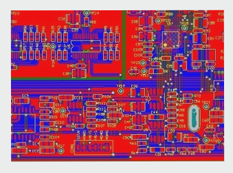
PCBA Foundry Material
Second, the process focus of PCBA foundry production
The technological emphasis in PCBA foundry production is crucial for mastering the related processes and methodologies. Understanding the key aspects of SMT patch proofing is akin to grasping the essence of SMT technology. Regardless of how complex or variable the soldering issues encountered may be, PCBA factories can effectively analyze and resolve problems in a targeted manner.
For instance, if one does not recognize that the BGA soldering process on a PCB involves both collapse and deformation during small batch SMT proofing, it becomes challenging to comprehend the significance of peak temperature and soldering duration. Additionally, if there is a lack of awareness that the properties of lead solder paste differ from those of lead-free BGA, understanding the complexities of the mixing process becomes difficult.
Thus, grasping the key points of PCB processing while learning SMT patch processing technology is essential. This foundational knowledge is vital for analyzing and addressing complex SMT patch proofing challenges. Surface assembly soldering technology, specifically the SMT patch proofing process, is intricate and continuously evolving—from leaded to eco-friendly lead-free processes, and from large to micro-pad soldering. Despite ongoing advancements in PCB processing, the fundamental principles remain unchanged.
Mastering the essential processes of PCBA production, along with understanding the causes and solutions for common soldering issues, can enhance the maturity and stability of SMT patch technology, establishing an effective quality control system. This knowledge is practically significant for swiftly addressing SMT processing and production technology challenges.

