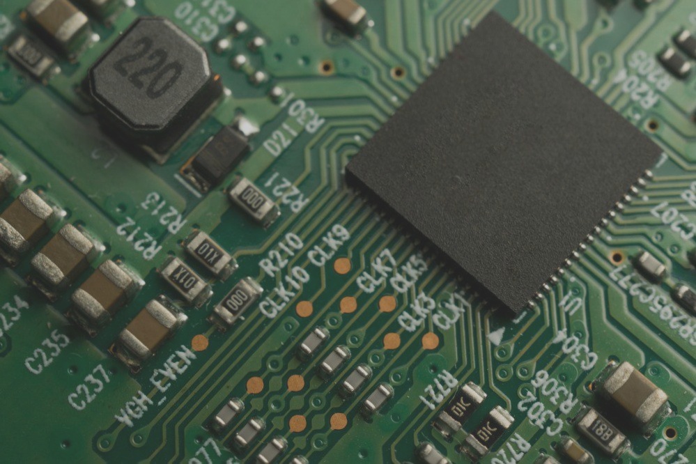
The Benefits of Microporous HDI PCB Production
- High path density with fewer layers due to small traces and vias
- Effective use of patterns with micro-holes for more space and open circuits
- Accommodation of multiple large and fine-pitch BGAs with spacing of 0.8 mm or less
Cost-Effective High-Frequency, High-Density Circuit Boards
HDI technology offers suitable laminated resolution, enhancing power and signal integrity for high-frequency PCBs. Newer materials can provide higher performance at a lower cost, but are not suitable for standard laminate processes.
The HDI Type II Structure
- Incorporates micro-holes, blind holes, and buried holes on the laminated core
- At least one layer of micro-holes on one or both sides
- Options to stagger, stack, or position microvias in relation to buried vias
Advantages of Type II HDI PCBs
Type II laminates are superior for densely packed boards with fine-pitch components, but face limitations similar to Type I due to core layer constraints.
Considerations for Type II HDI PCB Production
- Limitations on using outermost layer for grounding or power supply due to micro-holes
- Efficiency challenges when only one stacked layer is used for trace routing
About WellCircuits Limited
WellCircuits Limited specializes in high-precision circuit boards, including HDI, thick copper, backplanes, rigid-flex combinations, and more, to meet diverse customer needs.