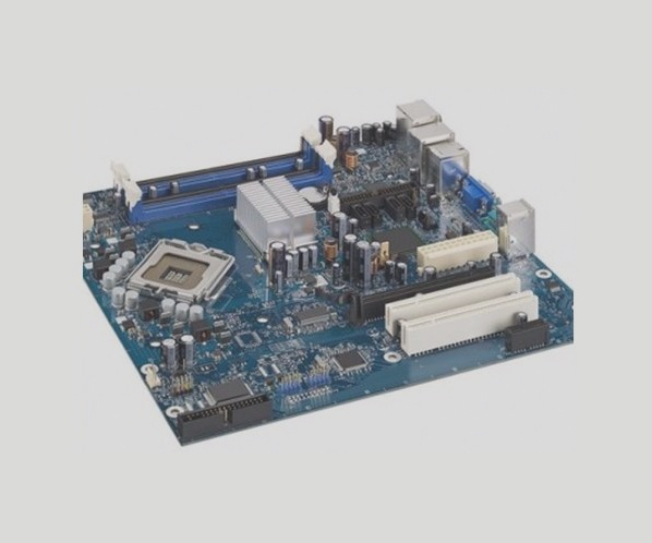
The Evolution of PCB Technology: Multilayer PCBs
The traditional printed circuit board (PCB) has evolved to meet the demands of complex circuits and applications. Initially composed of non-conductive substrate material like glass fiber epoxy and conductive layers of copper, modern PCBs now utilize multilayer technology for enhanced functionality.
Advantages of Multilayer PCBs
- Increased Circuit Density: Multilayer PCBs allow for more components in a smaller space, ideal for compact devices.
- Enhanced Performance: Improved signal integrity and reduced interference between components.
- Improved Reliability: Reduced physical damage risks, especially for high-density applications.
- Cost-Effectiveness: Economical for mass production of electronic products.
- Design Flexibility: Enables complex circuit design without sacrificing board space.
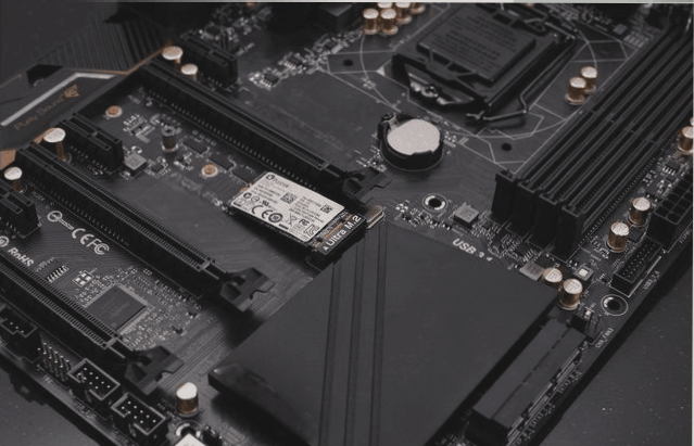
Space Requirements for Multi-Layer PCBs
Adding layers to a PCB minimally increases thickness, providing space-saving advantages for electronic products. This is crucial for modern electronics where space optimization is essential.
Weight Considerations
Multi-layer PCBs offer substantial weight reduction, benefiting portable devices like smartphones and laptops. The lightweight design supports device miniaturization without compromising performance.
Reliability and Consistency
Multi-layer PCB construction enhances reliability by minimizing signal interference and circuit failure risks. This is particularly important for high-performance electronic systems.
Disadvantages of Multi-Layer PCBs
Challenges and Considerations in Multi-Layer PCB Manufacturing
- Cost: One significant drawback of multi-layer PCBs is their higher manufacturing cost. The specialized equipment needed for production leads to a more expensive end product compared to single or double-sided boards. However, advancements in technology have reduced this cost gap, making multi-layer PCBs more accessible.
- Design Complexity: Creating intricate designs for multi-layer PCBs involves complex software tools and an understanding of advanced design principles. Engineers must adapt to specialized software, which requires training and a learning curve. This complexity can prolong the design process and raise the risk of errors if not managed correctly.
- Repair and Replacement Challenges: Due to the complex nature of multi-layer PCBs, fixing faults can be challenging, and sometimes impossible. When failures occur, replacing the entire board is often more cost-effective than attempting repairs, increasing the product’s overall lifecycle cost.
Factors Impacting Multi-Layer PCB Manufacturing
Manufacturing multi-layer PCBs demands specialized facilities and expertise. Not all PCB manufacturers have the capability to produce multi-layer boards due to the precise handling required for multiple layers, including copper foil, core materials, and prepreg layers. The layers are stacked, heated, and pressed together to form a cohesive structure. Specialized equipment and trained operators are essential for this process, which carries significant economic considerations.
Technological advancements have played a crucial role in supporting the design and production of multi-layer PCBs. Modern software tools, such as PCB design software, Design for Manufacturing (DFM) tools, and Computer-Aided Manufacturing (CAM) software, have streamlined the design process, enhanced manufacturability, and automated production verification.
These advancements have made multi-layer PCB design and manufacturing more efficient, leading to quicker turnaround times, reduced costs, and improved reliability. The increased adoption of multi-layer PCBs across various industries has resulted in more compact, durable, and cost-effective electronic devices.
Despite the benefits multi-layer PCBs offer in terms of space, weight, and reliability, considerations regarding costs, design complexity, and manufacturing capabilities are crucial. Ongoing technological progress continues to address these challenges, making multi-layer PCBs increasingly suitable for diverse applications.
If you have inquiries about PCB or PCBA, don’t hesitate to contact me at info@wellcircuits.com.