PCB Design Process
- Identify the functions required for the product.
- Develop a design plan and list all necessary components.
- Create a component symbol library based on the component list.
- Design a schematic diagram using the component symbol library and simulate it.
- Create a component package library based on physical component dimensions.
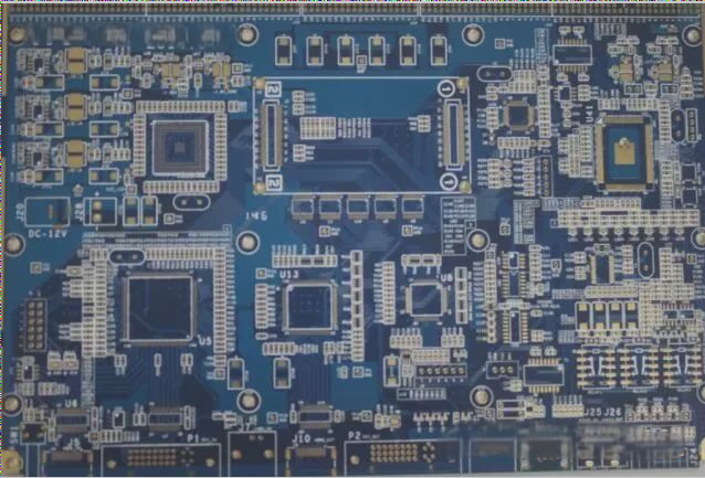
- Draw the PCB layout based on the schematic diagram.
- Prototype the PCB.
- Perform soldering, debugging, testing, and iterate if needed.
PCB design is a crucial phase in electronic product development. It involves translating schematic diagrams into physical circuit boards where components are mounted. The logical connections on the schematic are realized through copper traces on the PCB.
What is PCB?
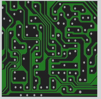
A Printed Circuit Board (PCB) is an insulating substrate with conductive patterns and holes for electrical connections between components. PCBs ensure repeatability, predictability, and easy testing of signals without short circuits. They support high-density installations and reliability, especially with Surface Mount Device (SMD) technology.
Development of Printed Boards
Printed circuit technology has roots dating back to the 19th century, evolving from simple resistors to complex multilayer boards. Dr. Paul Eisler’s work in the UK laid the foundation for modern PCBs. The 1950s saw advancements like high-adhesion copper-clad laminates, leading to mass production.
PCB Principles
PCBs provide mechanical support, enable electrical connections, maintain circuit characteristics, and aid in component location marking for easier maintenance.
Types of Printed Boards
Types of Printed Circuit Boards (PCBs)
-
Single-Sided Printed Board
A single-sided printed board has conductive patterns on one side only, with a thickness ranging from 0.2 to 5.0 mm. It is commonly used in electronic devices with basic requirements.
-
Double-Sided Printed PCB
Double-sided printed PCBs feature conductive patterns on both sides, with a thickness range of 0.2 to 5.0 mm. They are suitable for higher-performance electronic equipment.
-
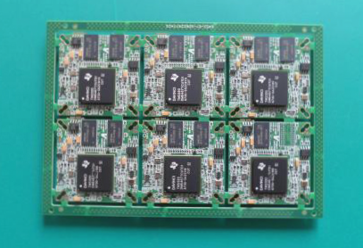
Multilayer Printed Boards
Multilayer printed boards consist of multiple layers of conductive and insulating materials, providing shorter and straighter connection paths. They are commonly used in computer cards for their advanced circuit capabilities.
Recent Developments:
Recent advancements in PCB technology have led to the development of flexible PCBs, also known as flex PCBs. These boards offer the advantage of being able to bend and twist, making them ideal for applications where traditional rigid PCBs are not suitable. Flex PCBs are commonly used in wearable devices, medical equipment, and aerospace applications.