Certainly! Can you specify which aspects of the article you’re most concerned about? For example, are you focusing on technical accuracy, readability, or something else?

**Layer stacking**: High-speed wiring typically requires stripline or microstrip layer configurations. These configurations provide a shielding layer for sensitive trace routing, helping to prevent EMI issues and maintain circuit signal integrity. Before starting the layout, you should agree on the layer stacking with your PCB contract manufacturer to establish a solid foundation and ensure manufacturability.
**Design rules**: Beyond standard trace width and spacing rules, high-speed design introduces a new set of rules and constraints. These include specifications for network types, differential pairs, trace length and topology, and impedance-controlled routing. There may also be specific requirements for blind and buried vias, micro vias, and other high-speed considerations.
Once these aspects are addressed, you can begin the PCB layout.
**Layout and routing techniques for high-speed PCB design**
Although there are many high-speed wiring technologies to consider, the first topic is component placement. Effective wiring starts with a good component layout, regardless of whether the board is designed for high speed.
**Component placement**
Utilize standard component placement methods, starting with connectors and large CPU and memory devices. To achieve optimal signal paths, continue placing parts according to the schematic’s logic flow. Many crucial CPU and memory devices will require numerous bypass capacitors, so place them promptly to avoid space issues later. When placing components, ensure space is reserved for routing channels and vias throughout the board stack. In addition to high-speed requirements, the placement must comply with design for manufacturability (DFM) rules and account for heat dissipation needs.
**Escape route**
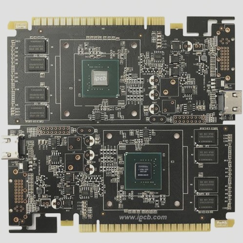
Before laying traces, create escape routes for all fine-pitch devices. For large components, such as BGAs with hundreds or thousands of pins, you need access to each pin for routing, often achieved by routing diagonally from the external pin row to the through hole. For the next row of pins, use very short traces to connect to the through holes between BGA pads, often referred to as dog-bone patterns. If the BGA pin pitch is very fine, you might need to use vias, micro vias, or both, but obtain manufacturer approval for these PCB technologies first. Component manufacturers usually provide recommended wiring patterns for their parts, so consult these to save time.
**Trace route**
After completing the escape routing, proceed with routing the remaining board. If design rules are fully set up, use automatic interactive routing tools or batch routing tools for manual completion. Regardless of the method, keep the following points in mind to ensure successful routing:
– High-speed signal paths should be kept short and routed directly from point to point.
– Sensitive traces should be routed on inner layers sandwiched between reference planes in a stripline configuration.
– Differential pairs must be routed in pairs. Use your design system’s automation features to ensure pairs are not interrupted by vias or other obstacles.
– For network groups requiring matched lengths, start with the longest connection. Adjust the remaining networks to match the length of the first network routed, often achieved by adding a waveform or trombone topology to the trace, typically handled automatically by CAD tools.
– Avoid routing sensitive digital lines through noisy power supplies or analog circuit areas.
**Power and ground plane**
Designing an effective power distribution network (PDN) for high-speed PCBs is crucial for overall design success. High-speed components generate more noise due to their switching rates, managed by bypass capacitors. Additionally, the ground plane serves as the reference plane for signal return. Avoid routing sensitive traces where signal return paths are obstructed by dense via placement, board cuts, or split planes, as these issues can degrade signal integrity.
High-speed wiring involves more than just routing unique traces on the board. Many aspects of PCB layout are critical to high-speed design, starting with correct board setup with your PCB contract manufacturer before layout begins.
**Work with your PCB CM to achieve the best high-speed routing technology**
While older PCB designs can often be adapted by adjusting layer stacks, high-speed designs should start with well-defined stacks. PCB designers are generally familiar with various board layer configurations, but high-speed designs involve additional variables such as circuit board materials, controlled impedance wiring, layer pairs, and assembly processes. Consulting your PCB contract manufacturer is essential to ensure you use the most optimized layer configuration for your design.


