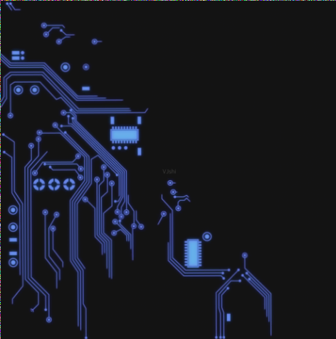
The specifications of modern electronic devices, such as wearable electronic devices, require PCB factories to adopt multi-layer HDI PCB buried blind via processing solutions. There are a large number of components on the surface even in PCB buried blind via processing, necessitating fine conductor widths and narrower spacing between them than conventional designs allow. Ordinary through holes will not fit in the available space, so manufacturers must use laser drilling for blind holes and embedded microvias.
Blind and buried via PCB factories are increasingly utilizing buried microvias to increase the number of interconnections in circuit boards while freeing up valuable space on the outer layer for more components. In addition to microvia technology and more layers, another aspect of advanced PCB buried blind hole processing is the trend towards thinner boards. Manufacturers are now employing thinner prepregs and cores compared to traditional designs.
As micro-equipment usage grows, PCB blind buried-via circuit board factories face pressure to produce complex PCBs. The production of HDI PCBs requires equipment similar to that used by traditional circuit board manufacturers, but with the added capability to handle small geometric shapes required for microholes.
For example, the use of HDI technology to manufacture complex PCBs with blind buried vias involves stacked multi-layer blind vias or embedded microvias. This process requires extra steps and repetition, increasing complexity and the risk of errors.
WellCircuits Limited specializes in high-precision double-sided, multi-layer, impedance-controlled, blind buried vias, and thick copper circuit boards. Their product range includes HDI, thick copper, backplanes, rigid-flex, buried capacitance, buried resistance, Golden Finger, and other types of circuit boards to meet customer demands for various products.


