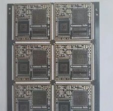
Enhancing PCB Density with Blind and Buried Hole Fabrication
As electronic products become more compact and precise, the demand for high-density circuit boards is increasing. One efficient way to achieve this is by reducing the number of through-holes and implementing accurate setups for blind and buried holes.
Understanding Blind and Buried Holes:
- Blind Holes vs. Through-Holes: Unlike through-holes that go through all layers, blind holes do not penetrate the entire depth of the board. In an eight-layer PCB, blind holes are divided into blind holes and buried holes (hidden within the board). During production, blind holes are drilled before pressing, while through-holes are drilled after pressing.
- Drill Belt:
- Reference Point Selection: Through-holes serve as reference points for the initial drilling belt.
- Coordination: Each blind hole drilling belt needs a specific hole marked in relation to the reference hole.
- Layer Identification: Consistent naming of drill belt layers is crucial for clarity in production.
Production Process for PCB Plates:
- Inner Layer Treatment: In multilayer boards, inner layers are left unperforated.
- Outer Layer Processing:
- Rivet Etching: Rivet GH, AOI GH, and ET GH are etched after drilling.
- Target Hole CCD: Outer layers require precise copper cutting and direct punching by X-Ray machines.
- Blind Hole Plate Considerations: Tooling holes, rivet GH, and beer-out are essential to prevent deviations. PNL plate edge production involves drilling holes for board identification.
- Film Processing: Positive film processing is preferred for plates thicker than 8mil, while thinner plates use negative processing. Copper thickness at D/F should be considered, and specific guidelines apply for blind hole applications.