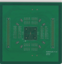
PCB surface blistering is a common quality defect in the PCB manufacturing process. The complexity of PCB production, especially during chemical wet treatments, makes it challenging to prevent blistering on the surface. Based on years of practical production and service experience, this article provides a brief analysis of the causes of blistering on the surface of copper electroplating circuit boards.
Blistering on the PCB surface is primarily caused by poor adhesion between the copper plating and the substrate, which leads to surface quality issues. These issues can be categorized into two key factors: 1) cleanliness of the board surface, and 2) surface micro-roughness (or surface energy). Essentially, all blistering problems can be traced back to these two factors. When adhesion between the plating layers is insufficient, it cannot withstand stresses that occur during subsequent manufacturing processes, such as coating stress, mechanical stress, and thermal stress. Over time, these stresses lead to separation between the layers of coating, causing blistering.
Several factors during PCB production and processing can contribute to poor board quality. These are summarized below:
1. **Inadequate Cleaning**: Any residual contaminants on the PCB surface, such as oils, dust, or oxidation, can prevent proper bonding between layers, resulting in blistering. Effective cleaning is essential at each step, especially before electroplating.
2. **Surface Micro-Roughness**: The quality of surface roughness is critical for ensuring strong adhesion between layers. Too smooth or too rough a surface can negatively affect the bonding strength, leading to delamination or blistering.
3. **Improper Chemical Treatment**: Variations in chemical concentrations or improper chemical treatment during the wet processes (e.g., etching, plating) can cause defects. For instance, insufficient activation of the copper surface or improper deposition of copper can weaken the adhesion layer.
4. **Temperature Fluctuations**: Thermal cycling during assembly, such as soldering, can induce stress on the PCB. If the copper layers are not sufficiently bonded to the substrate, thermal expansion and contraction can lead to blistering or delamination.
5. **Mechanical Stress**: During the handling, assembly, or testing phases, mechanical forces may cause deformation or stress on the PCB, leading to separation between the copper layers and the substrate.
In conclusion, preventing blistering defects requires careful attention to surface preparation, chemical treatments, and process control. Maintaining clean surfaces and optimizing micro-roughness levels are crucial for ensuring strong adhesion between layers. Additionally, managing thermal and mechanical stresses during manufacturing and assembly is essential for minimizing the risk of blistering.

### 1. Substrate Processing Challenges, Especially for Thin Substrates
Processing thin substrates, particularly those with a thickness below 0.8mm, presents unique challenges. Due to the low rigidity of these materials, brushing machines are often ineffective for cleaning, as they may not be able to remove contaminants effectively. Additionally, the thin protective layer on the copper foil, which is specifically designed to prevent oxidation during production, poses another issue. While this protective layer is delicate and could be removed by brushing, it is resistant to chemical treatments.
The primary concern here is to avoid damaging the surface of the substrate. Improper handling or processing can lead to blistering, caused by poor bonding between the base material copper foil and the chemical copper layer. This issue can also result in inconsistent blackening or browning during the inner layer blackening process, leading to uneven color or partial defects. Therefore, controlling the substrate’s handling during production is critical to prevent surface issues and ensure uniform results.
### 2. Surface Contamination from Oils, Liquids, and Dust
Another common problem in PCB production is poor surface treatment caused by contamination during machining processes such as drilling, lamination, or milling. Oils, liquids, and dust particles can easily contaminate the board surface, affecting the quality of subsequent treatments like etching and plating. This contamination can interfere with the uniformity of surface coatings and cause adhesion issues with subsequent layers, leading to defects or poor performance of the final product.
To mitigate this, it is essential to maintain clean working conditions during the machining processes. Proper cleaning protocols, such as rinsing or using specialized cleaning agents, can help ensure the board surface remains free from contaminants, thus improving the quality of the surface treatment.
### 3. Challenges with PCB Copper Sinking Process and Brushing Plate
The sinking copper process is another critical area where issues can arise, especially if the brushing plate is not properly adjusted. Excessive pressure applied to the substrate during the copper sinking process can lead to deformation of the holes. This deformation can cause the hole copper foil to round off or even lead to leakage of the base material. Such issues can cause blistering during electroplating or tin spraying processes.
Even if the brushing plate does not cause direct leakage of the substrate, excessive pressure can increase the roughness of the copper in the holes. This can result in over-roughening during the microetching process, which introduces potential quality risks, such as poor adhesion or uneven coatings.
To address this, it is important to carefully control the brushing process. The brushing parameters, including pressure and brush speed, should be optimized through regular testing, such as wear scar tests and water film tests, to ensure they are set to ideal conditions. This will help prevent deformation, minimize roughness, and maintain the overall integrity of the substrate during the sinking copper process.
### Conclusion
In conclusion, controlling the substrate processing, avoiding surface contamination, and optimizing the brushing process are all essential steps in ensuring the quality of PCB production. By understanding and addressing these common issues, manufacturers can minimize defects and improve the overall performance and reliability of the final product. Regular testing and process adjustments are key to achieving consistent, high-quality results.
Blistering on the PCB surface is primarily caused by poor adhesion between the copper plating and the substrate, which leads to surface quality issues. These issues can be categorized into two key factors: 1) cleanliness of the board surface, and 2) surface micro-roughness (or surface energy). Essentially, all blistering problems can be traced back to these two factors. When adhesion between the plating layers is insufficient, it cannot withstand stresses that occur during subsequent manufacturing processes, such as coating stress, mechanical stress, and thermal stress. Over time, these stresses lead to separation between the layers of coating, causing blistering.
Several factors during PCB production and processing can contribute to poor board quality. These are summarized below:
1. **Inadequate Cleaning**: Any residual contaminants on the PCB surface, such as oils, dust, or oxidation, can prevent proper bonding between layers, resulting in blistering. Effective cleaning is essential at each step, especially before electroplating.
2. **Surface Micro-Roughness**: The quality of surface roughness is critical for ensuring strong adhesion between layers. Too smooth or too rough a surface can negatively affect the bonding strength, leading to delamination or blistering.
3. **Improper Chemical Treatment**: Variations in chemical concentrations or improper chemical treatment during the wet processes (e.g., etching, plating) can cause defects. For instance, insufficient activation of the copper surface or improper deposition of copper can weaken the adhesion layer.
4. **Temperature Fluctuations**: Thermal cycling during assembly, such as soldering, can induce stress on the PCB. If the copper layers are not sufficiently bonded to the substrate, thermal expansion and contraction can lead to blistering or delamination.
5. **Mechanical Stress**: During the handling, assembly, or testing phases, mechanical forces may cause deformation or stress on the PCB, leading to separation between the copper layers and the substrate.
In conclusion, preventing blistering defects requires careful attention to surface preparation, chemical treatments, and process control. Maintaining clean surfaces and optimizing micro-roughness levels are crucial for ensuring strong adhesion between layers. Additionally, managing thermal and mechanical stresses during manufacturing and assembly is essential for minimizing the risk of blistering.
### 1. Substrate Processing Challenges, Especially for Thin Substrates
Processing thin substrates, particularly those with a thickness below 0.8mm, presents unique challenges. Due to the low rigidity of these materials, brushing machines are often ineffective for cleaning, as they may not be able to remove contaminants effectively. Additionally, the thin protective layer on the copper foil, which is specifically designed to prevent oxidation during production, poses another issue. While this protective layer is delicate and could be removed by brushing, it is resistant to chemical treatments.
The primary concern here is to avoid damaging the surface of the substrate. Improper handling or processing can lead to blistering, caused by poor bonding between the base material copper foil and the chemical copper layer. This issue can also result in inconsistent blackening or browning during the inner layer blackening process, leading to uneven color or partial defects. Therefore, controlling the substrate’s handling during production is critical to prevent surface issues and ensure uniform results.
### 2. Surface Contamination from Oils, Liquids, and Dust
Another common problem in PCB production is poor surface treatment caused by contamination during machining processes such as drilling, lamination, or milling. Oils, liquids, and dust particles can easily contaminate the board surface, affecting the quality of subsequent treatments like etching and plating. This contamination can interfere with the uniformity of surface coatings and cause adhesion issues with subsequent layers, leading to defects or poor performance of the final product.
To mitigate this, it is essential to maintain clean working conditions during the machining processes. Proper cleaning protocols, such as rinsing or using specialized cleaning agents, can help ensure the board surface remains free from contaminants, thus improving the quality of the surface treatment.
### 3. Challenges with PCB Copper Sinking Process and Brushing Plate
The sinking copper process is another critical area where issues can arise, especially if the brushing plate is not properly adjusted. Excessive pressure applied to the substrate during the copper sinking process can lead to deformation of the holes. This deformation can cause the hole copper foil to round off or even lead to leakage of the base material. Such issues can cause blistering during electroplating or tin spraying processes.
Even if the brushing plate does not cause direct leakage of the substrate, excessive pressure can increase the roughness of the copper in the holes. This can result in over-roughening during the microetching process, which introduces potential quality risks, such as poor adhesion or uneven coatings.
To address this, it is important to carefully control the brushing process. The brushing parameters, including pressure and brush speed, should be optimized through regular testing, such as wear scar tests and water film tests, to ensure they are set to ideal conditions. This will help prevent deformation, minimize roughness, and maintain the overall integrity of the substrate during the sinking copper process.
### Conclusion
In conclusion, controlling the substrate processing, avoiding surface contamination, and optimizing the brushing process are all essential steps in ensuring the quality of PCB production. By understanding and addressing these common issues, manufacturers can minimize defects and improve the overall performance and reliability of the final product. Regular testing and process adjustments are key to achieving consistent, high-quality results.