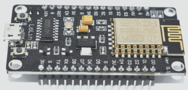
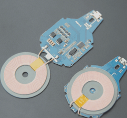
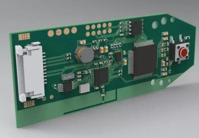
Cadence tools encompass both PCB assembly and PCB design components. To begin learning about PCB design components, it’s beneficial to compare them with Altium (formerly Protel). Cadence’s PCB assembly employs discrete tools, distinguishing it from Altium. With version 16.x as the standard, it incorporates nearly 10 key components.
Consideration of PCB assembly footprints occurs during the layout stage, where decisions on pad patterns and spatial occupation are crucial. These decisions impact the schematic drawing phase significantly. It’s essential to note that the footprint determination includes the mechanical dimensions of the components and their electrical pad connections.
This involves the pins fixed to the printed circuit board and the overall outline of the PCB assembly. Therefore, when selecting components, it’s important to consider any packaging or enclosure constraints that may affect both the top and bottom layers of the final PCB.
For instance, components like polarized capacitors often have specific clearance requirements that must be factored into the component selection process. When beginning the layout design, it may be necessary to first sketch a basic board outline and then place connectors or other critical components accordingly. This approach allows for the creation of a preliminary PCB visualization that is both efficient and eliminates the need for subsequent rewiring.
This preliminary visualization can then be refined to provide an accurate representation of component heights and their relative positions on the board. This ensures that once the PCB is assembled, all mechanical frameworks, chassis elements, and plastics can be properly accommodated within the package.

2. Prepare for Change
The selection of components may vary across different designs as the design process evolves. Consideration should be given to employing surface mount technology versus plated-through hole technology for different components. Pre-selecting the PCB design route can streamline the entire planning process. Before finalizing the PCB assembly, factors such as power consumption, component density, cost, and availability must be carefully evaluated.
Generally, surface mount technology components are more accessible and easier to procure compared to their plated-through hole counterparts. Moreover, from a manufacturing perspective, they often prove more cost-effective.
Interestingly, for medium and small-scale prototyping tasks, it is advisable to utilize larger through-hole components or surface mount technology components. This facilitates easier access to signals and pads during debugging and troubleshooting processes, and can simplify manual soldering operations. Additionally, if a specific footprint isn’t available in the database, custom footprint design tools can be utilized.
3. Implement Good Grounding Practices
Ensure that your design incorporates an adequate number of ground planes and bypass capacitors. When using integrated circuits (ICs), ensure the appropriate placement of decoupling capacitors near the power supply and ground planes.
The size of capacitors chosen should depend largely on the frequency involved, capacitor technology, and application type. Ultimately, adhering to good grounding specifications is crucial for optimizing magnetic characteristics and ensuring excellent electromagnetic compatibility of your printed circuit board.
4. Assign Virtual Part Footprints Correctly
It is strongly recommended to run a bill of materials (BOM) to verify the presence of any virtual components in your PCB design. Virtual components lack physical encapsulation and therefore do not translate into the layout phase. Reviewing the BOM allows for comprehensive evaluation of all virtual parts within the design.
During input, only ground and power signals should be entered, as these are specifically managed as virtual components in the schematic environment rather than the layout environment. To summarize, any virtual parts found in the PCB design should be replaced with components that have physical footprints, unless they are strictly for simulation purposes.
5. Check Unused Ports
To prevent floating inputs, ensure that all unused ports in your PCB design are correctly tied to a signal. Occasionally, PCB designs may inadvertently overlook or omit these unused ports, necessitating careful inspection to secure any unconnected inputs. Though uncommon, floating inputs can potentially lead to significant issues, such as failure of the entire system to operate as expected.
Consideration of PCB assembly footprints occurs during the layout stage, where decisions on pad patterns and spatial occupation are crucial. These decisions impact the schematic drawing phase significantly. It’s essential to note that the footprint determination includes the mechanical dimensions of the components and their electrical pad connections.
This involves the pins fixed to the printed circuit board and the overall outline of the PCB assembly. Therefore, when selecting components, it’s important to consider any packaging or enclosure constraints that may affect both the top and bottom layers of the final PCB.
For instance, components like polarized capacitors often have specific clearance requirements that must be factored into the component selection process. When beginning the layout design, it may be necessary to first sketch a basic board outline and then place connectors or other critical components accordingly. This approach allows for the creation of a preliminary PCB visualization that is both efficient and eliminates the need for subsequent rewiring.
This preliminary visualization can then be refined to provide an accurate representation of component heights and their relative positions on the board. This ensures that once the PCB is assembled, all mechanical frameworks, chassis elements, and plastics can be properly accommodated within the package.

2. Prepare for Change
The selection of components may vary across different designs as the design process evolves. Consideration should be given to employing surface mount technology versus plated-through hole technology for different components. Pre-selecting the PCB design route can streamline the entire planning process. Before finalizing the PCB assembly, factors such as power consumption, component density, cost, and availability must be carefully evaluated.
Generally, surface mount technology components are more accessible and easier to procure compared to their plated-through hole counterparts. Moreover, from a manufacturing perspective, they often prove more cost-effective.
Interestingly, for medium and small-scale prototyping tasks, it is advisable to utilize larger through-hole components or surface mount technology components. This facilitates easier access to signals and pads during debugging and troubleshooting processes, and can simplify manual soldering operations. Additionally, if a specific footprint isn’t available in the database, custom footprint design tools can be utilized.
3. Implement Good Grounding Practices
Ensure that your design incorporates an adequate number of ground planes and bypass capacitors. When using integrated circuits (ICs), ensure the appropriate placement of decoupling capacitors near the power supply and ground planes.
The size of capacitors chosen should depend largely on the frequency involved, capacitor technology, and application type. Ultimately, adhering to good grounding specifications is crucial for optimizing magnetic characteristics and ensuring excellent electromagnetic compatibility of your printed circuit board.
4. Assign Virtual Part Footprints Correctly
It is strongly recommended to run a bill of materials (BOM) to verify the presence of any virtual components in your PCB design. Virtual components lack physical encapsulation and therefore do not translate into the layout phase. Reviewing the BOM allows for comprehensive evaluation of all virtual parts within the design.
During input, only ground and power signals should be entered, as these are specifically managed as virtual components in the schematic environment rather than the layout environment. To summarize, any virtual parts found in the PCB design should be replaced with components that have physical footprints, unless they are strictly for simulation purposes.
5. Check Unused Ports
To prevent floating inputs, ensure that all unused ports in your PCB design are correctly tied to a signal. Occasionally, PCB designs may inadvertently overlook or omit these unused ports, necessitating careful inspection to secure any unconnected inputs. Though uncommon, floating inputs can potentially lead to significant issues, such as failure of the entire system to operate as expected.


