
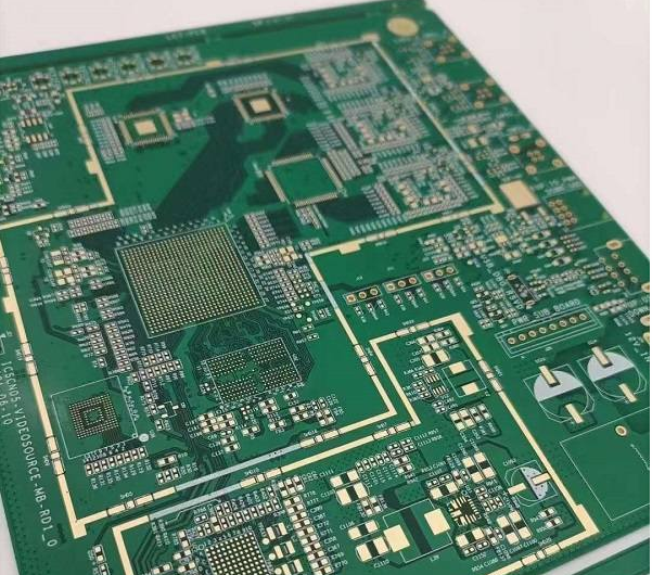
Understanding Crosstalk in PCBs
Causes of Crosstalk
When signals travel along PCB traces, electromagnetic waves induce voltages and currents in adjacent traces due to electromagnetic induction. This phenomenon, governed by Maxwell’s equations, leads to crosstalk, where signals are generated in neighboring lines.
Capacitance Characteristics of Forward Crosstalk
Forward crosstalk exhibits capacitive and inductive characteristics. The coupling capacitance between wires influences the amplitude of crosstalk pulses, with factors like PCB material and line positioning playing a role. Inductive characteristics come into play, with the polarity of forward crosstalk signals opposite to capacitive crosstalk.
Inductive vs. Capacitive Crosstalk
- Inductive crosstalk cancels out capacitive crosstalk when equal, preventing forward crosstalk.
- Backward crosstalk, prevalent in long strip circuit boards, exhibits different characteristics from forward crosstalk.
- The amplitude of backward crosstalk pulses is independent of line length, with a duration double the delay time of the “intrusion” signal.
By understanding the distinctions between forward and backward crosstalk, PCB designers can mitigate signal interference effectively.
Understanding and Mitigating Crosstalk Interference in PCB Design
- When designing PCBs, it’s crucial to consider both forward and backward crosstalk interference between driver and receiver chips.
- Backward crosstalk, with a single polarity, can’t cancel itself out like forward crosstalk, making it important to address.
- Measuring backward crosstalk accurately is essential, as it reflects back from the “victim” driver chip.
- Quantitative metrics are vital in digital design, with a maximum noise tolerance of 150mV for crosstalk.
- Modifying geometric parameters and using multi-line terminals can help mitigate crosstalk effectively.
- Reducing line length and increasing distance between coupled lines are strategies to consider.
- Layering methods, dielectric material thickness, and impedance array terminals play key roles in minimizing crosstalk interference.
- While challenges exist, impedance array terminals are recommended for addressing crosstalk in PCB designs.
By understanding the complexities of crosstalk interference and implementing effective mitigation strategies, PCB designers can enhance signal integrity and overall performance in high-speed circuit designs.
 العربية
 简体中文
简体中文 Nederlands
 English
 Français
 Deutsch
 Italiano
 日本語
日本語 한국어
한국어 Português
 Русский
 Español
 ไทย
ไทย