Understanding PCB Layers and Materials in Modern Technology
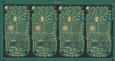
Printed Circuit Boards (PCBs) play a crucial role in today’s technology-driven world, providing essential platforms for large-scale integrated circuits. In the past, there was a common misconception in the DIY industry that more layers in a PCB equated to better performance. However, this belief is unfounded. Additional PCB layers are typically added as a last resort due to physical constraints, when double-layer wiring is insufficient to accommodate the circuitry.
Contrary to popular belief, multi-layer PCBs come at a higher cost and do not always translate to more cost-effective products. The number of layers in a PCB is determined by specific factors, rather than a simple “more is better” approach.

As technology advances, electronic components are becoming more integrated, leading to a decrease in the number of layers in motherboard PCBs. The materials used in PCB fabrication are also evolving towards higher integration. For instance, modern LCD TVs are thinner and offer better display quality compared to older CRT TVs, showcasing the progress in PCB technology.
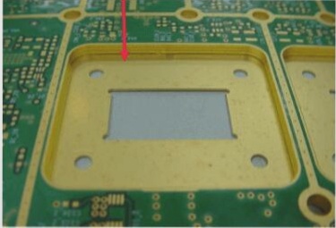
Currently, the predominant material used in PCB manufacturing is glass fiber. A simple way to identify a high-quality PCB is by its smooth and flat surface, indicating superior craftsmanship. In contrast, rough PCBs may be constructed from fire-resistant cardboard, which signifies lower quality.
While a good PCB board doesn’t necessarily have to be extremely hard, it should exhibit toughness and the ability to quickly regain its original shape after gentle bending. Avoid testing the strength of a motherboard by applying excessive force, as it may lead to damage beyond the scope of warranty coverage.