Creating Unique PCB Designs Without Traditional Component Placement
Are you looking to design a PCB with a non-standard shape without the need to place individual components first in EDA software? Wondering if it’s possible and which software would be best suited for this task? Let’s explore.
Breaking Away from Traditional Methods
If you’re new to PCB design and want to break away from the conventional process of placing components individually, you’re not alone. Many hobbyists face similar challenges when trying to create custom PCBs with unique shapes.
Typically, EDA software follows a specific order of operations, starting with placing individual components, defining connections, creating schematics, and finally running traces to ensure everything works seamlessly. However, when dealing with complex systems like Raspberry Pi, Arduino, and power supplies, the traditional approach may not be the most efficient.
Streamlining Your Design Process
Imagine a PCB where all your off-the-shelf systems are seamlessly integrated, eliminating the need for excessive wiring and bulky setups. By soldering components like Raspberry Pi, Arduino, and power supplies directly onto the PCB, you can create a compact and efficient solution.
But how do you find software that accommodates these unique requirements? Look for tools that offer a diverse component library, allowing you to treat entire systems as individual components. This way, you can place and connect complex modules like Arduino and power supplies with ease, ensuring precise alignment and spacing.
Defining Unconventional Shapes
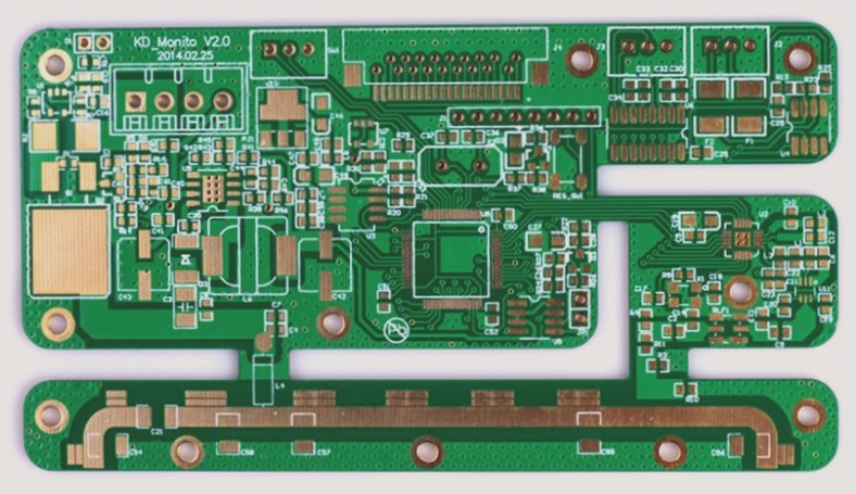
Designing a PCB with an atypical shape presents its own set of challenges. Whether you need cutouts for cooling fans, protrusions for heat sinks, or specific dimensions to fit within a shell, finding the right software is crucial.
Look for software that allows you to define custom shapes with precision. Whether it’s creating cutouts for components, adding holes for mounting, or incorporating unique features like button protrusions, the software you choose should offer the flexibility to bring your unconventional designs to life.
By selecting the right tools and embracing a creative approach to PCB design, you can overcome traditional constraints and unleash your full potential in creating innovative and functional circuit boards.
Creating Custom PCB Shapes with Silk Screen Lines
When faced with challenges in PCB design, one possible solution is to design the overall rectangle size of the board, incorporating silk screen lines that outline areas to be cut out. By using a dremel to remove these sections, while ensuring that all traces stay within the designated boundaries, you can achieve the final desired shape. This approach can be particularly beneficial for the initial prototype version, allowing you to collect data and refine the dimensions accordingly.
Choosing the Right EDA Program for Custom PCB Designs
Are you wondering if customizing PCB shapes through silk screen lines is feasible, or if there is a specific EDA (Electronic Design Automation) program better suited for this task? Exploring different EDA software options can help you find the most suitable tool to bring your innovative PCB design ideas to life.