Uncategorized

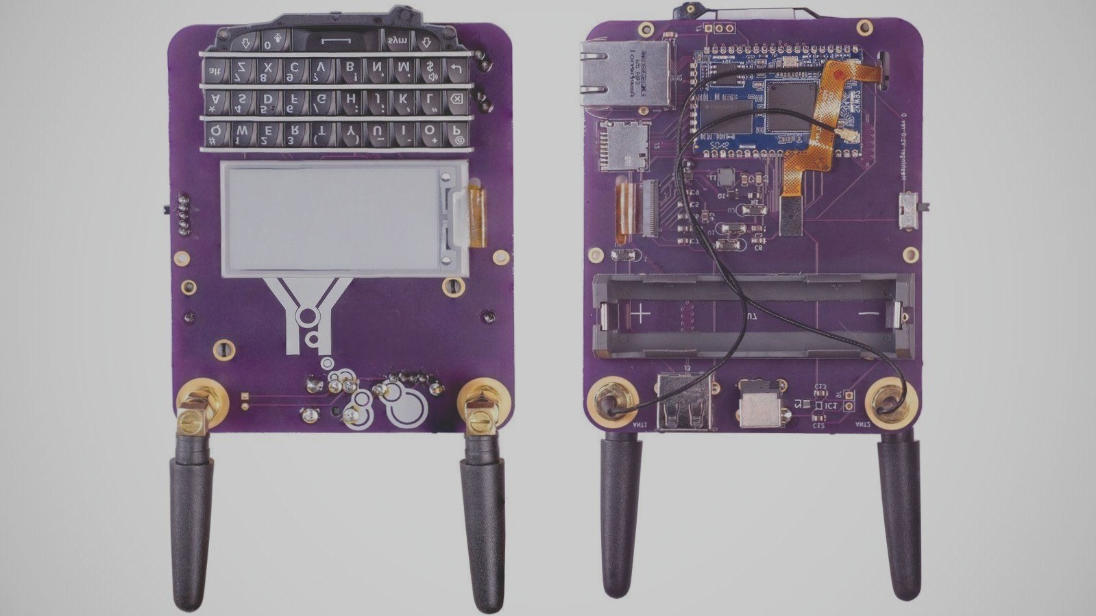
PCB reverse engineering focuses on key aspects such as component identification, layer structure analysis, and manufacturing process understanding.

In PCB reverse engineering, reconstructing the schematic involves dividing functional areas, identifying reference components, distinguishing different wire types, learning from similar designs, and reviewing the final schematic for accuracy and optimization to ensure it reflects the circuit’s operational principles.

PCB reverse engineering focuses on key aspects such as component identification, layer structure analysis, and manufacturing process understanding. Read More »

What is PCB design and how are integrated circuits incorporated into it?

A PCB consists of several key components such as circuits, dielectric layers, holes, solder resist, silk screens, and surface finishes, providing high-density, reliable, flexible, and testable designs, while integrated circuits (ICs) are small, high-performance chips soldered onto the PCB to enhance functionality and reliability.

What is PCB design and how are integrated circuits incorporated into it? Read More »

Principles of PCB Layout Design and Electromagnetic Interference Mitigation Techniques

A **Printed Circuit Board (PCB)** serves as the foundation for electronic circuits, and its design plays a crucial role in minimizing interference and optimizing performance, with key considerations including component placement, trace routing, and anti-interference measures.

Principles of PCB Layout Design and Electromagnetic Interference Mitigation Techniques Read More »

Essential Aspects of PCB Copper Cladding and CAD File Conversion

The article discusses the challenges and best practices involved in PCB copper cladding, CAD-to-Gerber file conversion, and related technical considerations, emphasizing efficient grounding, interference suppression, and proper file handling to avoid errors during manufacturing.

Essential Aspects of PCB Copper Cladding and CAD File Conversion Read More »

Principles of PCB Anti-Jamming Design

The guidelines for PCB power line layout emphasize optimizing power and ground trace width, proper decoupling capacitor placement, and careful separation of digital and analog grounds, while minimizing interference through proper component positioning, trace routing, and shielding techniques.

Principles of PCB Anti-Jamming Design Read More »

Automatic Detection Technology for PCB Manufacturing

Shen’an PCB Circuit Board Production Automatic Detection Technology outlines two common methods for PCB inspection: the needle bed test, which involves spring-loaded probes for testing multiple points simultaneously but is costly and difficult to maintain, and the flying probe test, which uses movable probes controlled by CAD data and is more suitable for low-volume, complex PCB production despite being slower and more expensive.

Automatic Detection Technology for PCB Manufacturing Read More »

The key considerations in PCB design

This article provides key guidelines for designing high-quality PCBs, covering essential factors like FPGA pin verification, layer stack-up, power distribution, signal routing, analog-digital isolation, iterative development, and effective layout strategies for minimizing interference and ensuring signal integrity.

The key considerations in PCB design Read More »

Introduction to Three Types of Holes for PCB Prototyping

The text explains the different types of vias used in PCB manufacturing—through holes, blind holes, and buried vias—each serving distinct purposes in connecting circuit layers, with varying levels of complexity, cost, and space utilization.

Introduction to Three Types of Holes for PCB Prototyping Read More »

Contact

WellCircuits
More than PCB

Upload your GerberFile(7z,rar,zip)