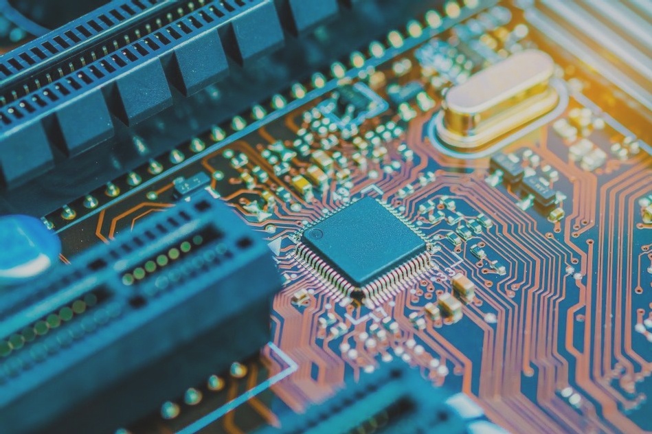
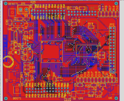
The wiring of a PCB board requires a high level of precision, and many manufacturers utilize the dry film process to transfer circuit graphics.
1. When the dry film has holes during masking, the following steps can be taken:
1) Reduce the film temperature and pressure;
2) Improve hole wall roughness and tip;
3) Enhance the energy of exposure;
4) Reduce the developing pressure;
5) Avoid leaving the film applied for too long to prevent diffusion and thinning of the semi-fluid film at the corners;
6) Ensure that the dry film is not overly tight during application.

2. Penetration during dry film electroplating is a common issue that occurs when the dry film and copper foil are not firmly adhered, allowing the electroplating solution to seep through. This issue can be caused by several factors:
1) Inappropriate film temperature
If the temperature is too low, the corrosion resistant film will not soften and flow sufficiently, resulting in poor adhesion. If the temperature is too high, rapid solvent volatilization will cause the dry film to become brittle, leading to warping and peeling during electroplating shock, resulting in penetration.
2) High or low film pressure
Low pressure can cause uneven surfaces or gaps between the dry film and copper plate, while excessively high pressure can lead to excessive solvent volatilization and brittleness in the dry film, resulting in peeling after electroplating.
3) High or low exposure energy
Insufficient exposure can cause incomplete polymerization, leading to swelling and softening of the adhesive film, while excessive exposure can lead to development difficulties and warping and peeling during electroplating, resulting in penetration.
3. Board surface blistering is a common quality defect in the PCB production process. There are several causes of blistering on the PCB surface:
1) Substrate processing issues
Thinner substrates may have poor rigidity, making it unsuitable to use a brush during processing, which can lead to poor adhesion between copper foil and chemical copper, causing surface blistering.
2) Oil stains and other contaminants
Machining processes and other liquids contaminated with dust can cause surface blistering on the PCB.
3) Poor copper brush plating
Excessive pressure during grinding before copper deposition can cause orifice deformation and subsequent blistering during the production process.
4) Water washing problems
Chemical solution treatments and various solvents can lead to cross-contamination and poor local treatment, affecting binding force.
5) Excessive micro etching
Over-etching can cause base material leakage at the orifice, resulting in blistering around the orifice.
6) Overly active copper precipitation solution
Newly opened cylinders or high component content in the bath of copper plating solution can lead to poor adhesion and physical property decline.
7) Oxidation during production
Board surface oxidation can cause blistering.
8) Poor copper reworking
Incorrect reworking methods or improper micro etching control can result in blistering during reworking.
9) Graphic transfer issues
Insufficient water washing after development, prolonged storage time, or excessive dust in the workshop can lead to potential quality problems.
10) Pickling tank maintenance
Inadequate maintenance of pickling tanks can lead to cleanliness and surface roughness issues.
11) Organic pollution in electroplating tanks
Oil contamination in electroplating tanks can cause blistering on the PCB surface.
12) Charged PCB board entry
Special attention should be paid to charged PCB boards entering tanks, especially in tanks with air agitation.
1. When the dry film has holes during masking, the following steps can be taken:
1) Reduce the film temperature and pressure;
2) Improve hole wall roughness and tip;
3) Enhance the energy of exposure;
4) Reduce the developing pressure;
5) Avoid leaving the film applied for too long to prevent diffusion and thinning of the semi-fluid film at the corners;
6) Ensure that the dry film is not overly tight during application.

2. Penetration during dry film electroplating is a common issue that occurs when the dry film and copper foil are not firmly adhered, allowing the electroplating solution to seep through. This issue can be caused by several factors:
1) Inappropriate film temperature
If the temperature is too low, the corrosion resistant film will not soften and flow sufficiently, resulting in poor adhesion. If the temperature is too high, rapid solvent volatilization will cause the dry film to become brittle, leading to warping and peeling during electroplating shock, resulting in penetration.
2) High or low film pressure
Low pressure can cause uneven surfaces or gaps between the dry film and copper plate, while excessively high pressure can lead to excessive solvent volatilization and brittleness in the dry film, resulting in peeling after electroplating.
3) High or low exposure energy
Insufficient exposure can cause incomplete polymerization, leading to swelling and softening of the adhesive film, while excessive exposure can lead to development difficulties and warping and peeling during electroplating, resulting in penetration.
3. Board surface blistering is a common quality defect in the PCB production process. There are several causes of blistering on the PCB surface:
1) Substrate processing issues
Thinner substrates may have poor rigidity, making it unsuitable to use a brush during processing, which can lead to poor adhesion between copper foil and chemical copper, causing surface blistering.
2) Oil stains and other contaminants
Machining processes and other liquids contaminated with dust can cause surface blistering on the PCB.
3) Poor copper brush plating
Excessive pressure during grinding before copper deposition can cause orifice deformation and subsequent blistering during the production process.
4) Water washing problems
Chemical solution treatments and various solvents can lead to cross-contamination and poor local treatment, affecting binding force.
5) Excessive micro etching
Over-etching can cause base material leakage at the orifice, resulting in blistering around the orifice.
6) Overly active copper precipitation solution
Newly opened cylinders or high component content in the bath of copper plating solution can lead to poor adhesion and physical property decline.
7) Oxidation during production
Board surface oxidation can cause blistering.
8) Poor copper reworking
Incorrect reworking methods or improper micro etching control can result in blistering during reworking.
9) Graphic transfer issues
Insufficient water washing after development, prolonged storage time, or excessive dust in the workshop can lead to potential quality problems.
10) Pickling tank maintenance
Inadequate maintenance of pickling tanks can lead to cleanliness and surface roughness issues.
11) Organic pollution in electroplating tanks
Oil contamination in electroplating tanks can cause blistering on the PCB surface.
12) Charged PCB board entry
Special attention should be paid to charged PCB boards entering tanks, especially in tanks with air agitation.


