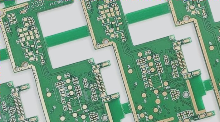
Looking back at the recent development of the electronic PCB board industry, a clear trend emerges: reflow soldering technology. Traditionally, even through-hole components can now be reflow soldered, known as through-hole reflow soldering. This method offers the advantage of simultaneously completing all solder joints, thereby minimizing production costs. However, the use of reflow soldering is limited by temperature-sensitive components, whether they are plug-in or SMD.
Subsequently, attention shifted to selective soldering. Selective soldering can complement reflow soldering in most applications. This approach offers an economical and efficient way to solder remaining through-hole components and is fully compatible with future lead-free soldering processes.

Process Characteristics of Selective Soldering
1. The process characteristics of selective soldering can be understood by comparing it with wave soldering. The most noticeable difference lies in how the solder interacts with the PCB. In wave soldering, the entire lower part of the PCB is submerged in liquid solder, whereas selective soldering targets specific areas, minimizing heat transfer to adjacent components and PCB regions. Additionally, flux must be applied prior to soldering. Unlike wave soldering, where flux covers the entire PCB, selective soldering restricts flux application to the designated soldering areas. Moreover, selective soldering is suitable only for through-hole components, representing a distinct and modern approach requiring comprehensive process and equipment understanding for successful implementation.
2. Typical Process of Selective Soldering
3. The typical selective soldering processes encompass flux spraying, PCB preheating, dip soldering, and drag soldering. Each stage plays a crucial role in ensuring effective soldering.
4. Flux Application Process
5. In selective soldering, the flux application process is pivotal. Effective flux application post-soldering ensures activity to prevent bridging and oxidation of the PCB. Flux is sprayed via an X/Y manipulator passing over the flux nozzle, precisely coating the intended PCB areas. Flux application methods include single nozzle spray, micro-hole spray, and synchronized multi-point/pattern spray. Accurate flux deposition post-reflow is critical, with micro-hole jets preventing unintended areas from being coated. The flux pattern’s diameter exceeds 2mm, ensuring ±0.5mm positional accuracy to consistently cover solder joints. Supplier-provided tolerance specifications ensure flux application remains within a 100% safety margin.
6. Preheating Process
7. Preheating serves primarily to evaporate flux solvents, adjusting viscosity for optimal interaction with the solder wave. It plays a secondary role in managing thermal stress during soldering, with settings determined by PCB thickness, device specifications, and flux type. There are differing views on preheating in selective soldering: some engineers advocate preheating before flux application, while others prefer direct soldering without preheating, allowing users to tailor processes based on specific needs.
8. Soldering Process
9. Selective soldering employs two primary techniques: drag soldering and dip soldering. Drag soldering utilizes a small-tip solder wave, ideal for tight PCB spaces such as individual joints or pins. Soldering quality is managed by adjusting PCB movement speed and angle relative to the solder wave, ensuring stability with tips under 6mm diameter. Solder nozzles are optimized for different orientations, with manipulator angles ranging from 0° to 12°, typically set at 10° for optimal performance. Compared to dip soldering, drag soldering offers enhanced heat transfer efficiency and reliability, aided by solder wave temperatures of 275℃ to 300℃ and drag speeds of 10mm/s to 25mm/s, supported by nitrogen supply to prevent oxidation and bridging defects, ensuring stable, high-quality solder joints.
10. Manipulator Capabilities
11. Selective soldering benefits from precise manipulator capabilities, featuring ±0.05mm positioning accuracy for consistent board parameters and a 5-dimensional movement range to optimize solder joint contact angles and orientations. Titanium alloy stylus-tipped solder wave height control enhances process stability via program-controlled measurement and pump speed adjustment.
12. Process Efficiency and Flexibility
13. Despite its advantages, single-nozzle drag soldering processes exhibit prolonged flux spraying, preheating, and soldering times. As solder joint counts increase, efficiency lags compared to traditional wave soldering. However, multi-tip designs boost throughput—dual-nozzle setups double output, complemented by dual-nozzle flux applications. Immersion selective soldering systems, though less flexible than robotic counterparts, match traditional wave soldering outputs at lower costs. They accommodate single or multi-board transfers, ensuring simultaneous fluxing, preheating, and soldering of all joints, albeit necessitating specialized nozzle designs based on PCB layouts.
14. Design Considerations
15. Designers prioritize large solder tip sizes to stabilize soldering processes without impacting adjacent PCB components. This design challenge underscores process stability’s critical role in selective soldering, supporting the soldering of 0.7mm to 10mm joints, favoring stability for short leads and small pad sizes, with a minimum 5mm spacing between adjacent solder joints, devices, and solder tips on PCBs.
Subsequently, attention shifted to selective soldering. Selective soldering can complement reflow soldering in most applications. This approach offers an economical and efficient way to solder remaining through-hole components and is fully compatible with future lead-free soldering processes.

Process Characteristics of Selective Soldering
1. The process characteristics of selective soldering can be understood by comparing it with wave soldering. The most noticeable difference lies in how the solder interacts with the PCB. In wave soldering, the entire lower part of the PCB is submerged in liquid solder, whereas selective soldering targets specific areas, minimizing heat transfer to adjacent components and PCB regions. Additionally, flux must be applied prior to soldering. Unlike wave soldering, where flux covers the entire PCB, selective soldering restricts flux application to the designated soldering areas. Moreover, selective soldering is suitable only for through-hole components, representing a distinct and modern approach requiring comprehensive process and equipment understanding for successful implementation.
2. Typical Process of Selective Soldering
3. The typical selective soldering processes encompass flux spraying, PCB preheating, dip soldering, and drag soldering. Each stage plays a crucial role in ensuring effective soldering.
4. Flux Application Process
5. In selective soldering, the flux application process is pivotal. Effective flux application post-soldering ensures activity to prevent bridging and oxidation of the PCB. Flux is sprayed via an X/Y manipulator passing over the flux nozzle, precisely coating the intended PCB areas. Flux application methods include single nozzle spray, micro-hole spray, and synchronized multi-point/pattern spray. Accurate flux deposition post-reflow is critical, with micro-hole jets preventing unintended areas from being coated. The flux pattern’s diameter exceeds 2mm, ensuring ±0.5mm positional accuracy to consistently cover solder joints. Supplier-provided tolerance specifications ensure flux application remains within a 100% safety margin.
6. Preheating Process
7. Preheating serves primarily to evaporate flux solvents, adjusting viscosity for optimal interaction with the solder wave. It plays a secondary role in managing thermal stress during soldering, with settings determined by PCB thickness, device specifications, and flux type. There are differing views on preheating in selective soldering: some engineers advocate preheating before flux application, while others prefer direct soldering without preheating, allowing users to tailor processes based on specific needs.
8. Soldering Process
9. Selective soldering employs two primary techniques: drag soldering and dip soldering. Drag soldering utilizes a small-tip solder wave, ideal for tight PCB spaces such as individual joints or pins. Soldering quality is managed by adjusting PCB movement speed and angle relative to the solder wave, ensuring stability with tips under 6mm diameter. Solder nozzles are optimized for different orientations, with manipulator angles ranging from 0° to 12°, typically set at 10° for optimal performance. Compared to dip soldering, drag soldering offers enhanced heat transfer efficiency and reliability, aided by solder wave temperatures of 275℃ to 300℃ and drag speeds of 10mm/s to 25mm/s, supported by nitrogen supply to prevent oxidation and bridging defects, ensuring stable, high-quality solder joints.
10. Manipulator Capabilities
11. Selective soldering benefits from precise manipulator capabilities, featuring ±0.05mm positioning accuracy for consistent board parameters and a 5-dimensional movement range to optimize solder joint contact angles and orientations. Titanium alloy stylus-tipped solder wave height control enhances process stability via program-controlled measurement and pump speed adjustment.
12. Process Efficiency and Flexibility
13. Despite its advantages, single-nozzle drag soldering processes exhibit prolonged flux spraying, preheating, and soldering times. As solder joint counts increase, efficiency lags compared to traditional wave soldering. However, multi-tip designs boost throughput—dual-nozzle setups double output, complemented by dual-nozzle flux applications. Immersion selective soldering systems, though less flexible than robotic counterparts, match traditional wave soldering outputs at lower costs. They accommodate single or multi-board transfers, ensuring simultaneous fluxing, preheating, and soldering of all joints, albeit necessitating specialized nozzle designs based on PCB layouts.
14. Design Considerations
15. Designers prioritize large solder tip sizes to stabilize soldering processes without impacting adjacent PCB components. This design challenge underscores process stability’s critical role in selective soldering, supporting the soldering of 0.7mm to 10mm joints, favoring stability for short leads and small pad sizes, with a minimum 5mm spacing between adjacent solder joints, devices, and solder tips on PCBs.


