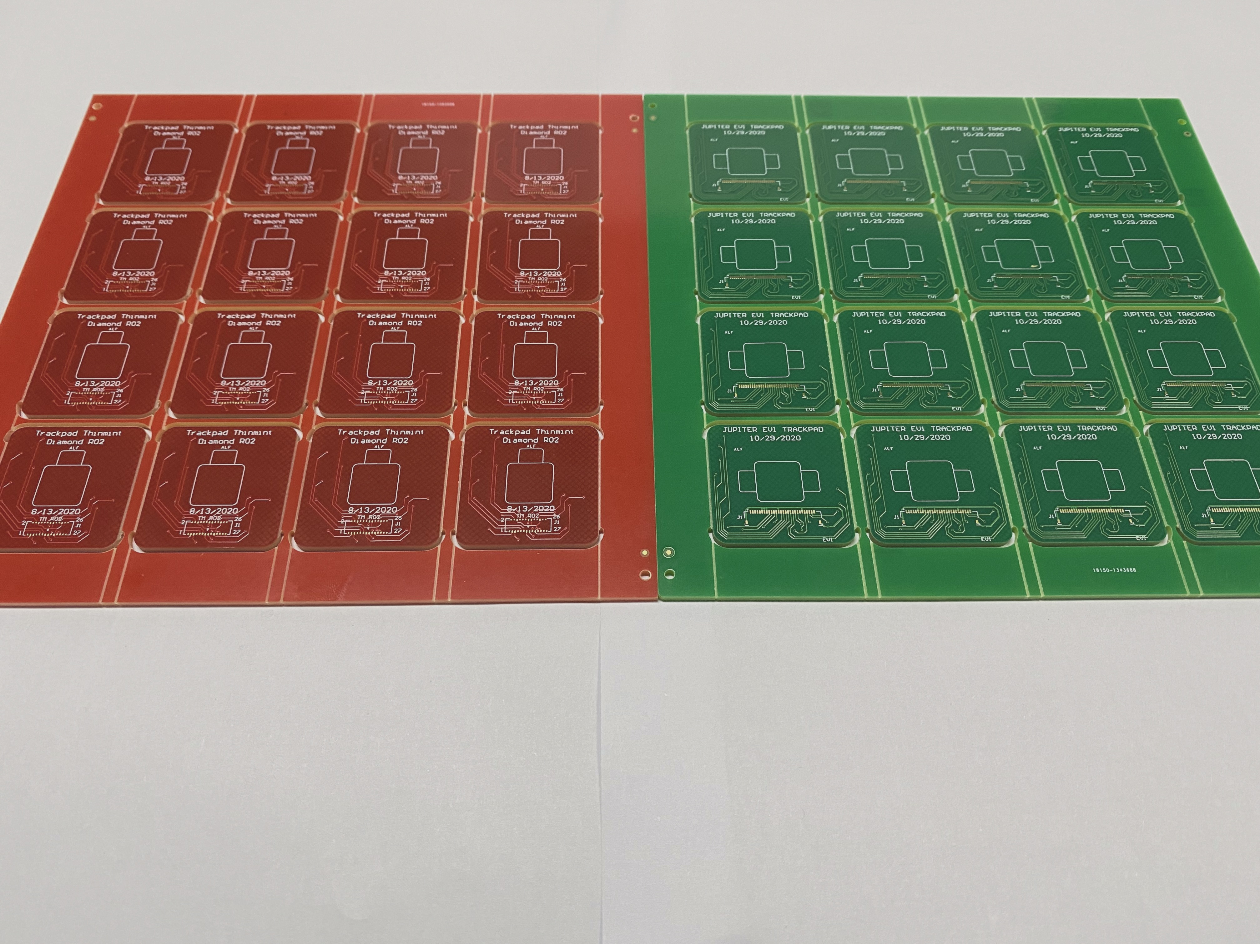
Causes of PCB Solder Mask Ink Shedding
PCB solder mask ink refers to the surface ink color layer printed during PCB board customization. Issues like inadequate thickness, exposure to chemicals, and trace thickness can lead to ink shedding.
Factors Contributing to PCB Solder Mask Ink Shedding:
- Inadequate pre-process treatment
- Insufficient baking after ink printing
- Poor quality ink
Under normal conditions, double-sided boards are more prone to pad detachment compared to single-sided boards. Multi-layer boards have lower detachment rates due to rapid heat dissipation.
Causes of Pad Detachment During Soldering:
- Repeated soldering
- Excessive soldering iron temperature
- Excessive pressure and prolonged soldering time
To prevent pad detachment, measures include increasing solder joints, enhancing PCBA pad solderability, improving soldering processes, and employee proficiency.
Selection of PCB Substrates
Optimal selection of materials and pressing processes for PCB substrates can prevent solder mask ink detachment. Desiccants are used to maintain circuit board dryness during storage and transit.