Annular Ring
The annular ring, a copper ring surrounding the through-hole on a PCB surface, is crucial for maintaining electrical continuity in multi-layer PCBs. It serves as a connection point for traces, an endpoint for signal routing, and even a soldering pad for component leads. Terms like “pad,” “land,” and “via pad” are related to the annular ring, highlighting its importance in professional PCB design.
Artwork Film
Artwork film, black-and-white negatives used in photolithography, transfers PCB designs onto copper substrates. Master artwork contains the original layout, while working artwork is re-photographed for reproducing designs. Though technology has evolved, understanding the historical significance of artwork films remains crucial in PCB manufacturing.
Basic Grid
The basic grid, a reference system in PCB design, determines horizontal and vertical spacing for components, traces, and vias. Originally 100 mils, grid spacing now goes down to 50 mils or smaller for high-density designs. This grid is vital for consistent design, proper component spacing, efficient routing, and reliable signal integrity in high-speed circuits.
Blind Via Hole
A blind via hole, a specialized type of via in multi-layer PCBs, connects specific internal layers without penetrating the entire board. It may terminate at an outer layer without fully penetrating, conserving space and simplifying drilling operations. Blind vias are essential in high-density designs for space conservation and improved signal integrity.
Summary
Understanding technical terms like annular rings, artwork films, basic grids, and blind via holes is essential in creating high-performance PCBs. These elements contribute to proper component placement, signal routing, and layer interconnection. As PCB technology advances, staying updated with these terms and their applications is crucial for designers and manufacturers.
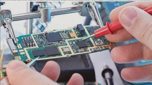
PCB Assembly and Component Representation
A block diagram visually represents the assembly board and its components, using electrical symbols to show how these components are interconnected. This method aids in understanding the system architecture and component relationships during the design and assembly process.
Bomb Sight (Bullet Mark)
In PCB production, a “Photographers’ Target” system is utilized, similar to the aiming screen used by bombers. Alignment targets placed at each corner of the PCB ensure precise layer alignment between the top and bottom layers of the board.
Break-Away Panel (Disconnection Panel)
Break-away panels are employed in PCB manufacturing to simplify handling and assembly. Small circuit boards are combined onto a larger board for processing, with tie bars or break-away tabs holding them together. These tabs allow for easy separation post-assembly, enhancing efficiency in operations.
Buried Via Hole
Within multi-layer PCBs, buried vias are crucial for routing signals and power connections between internal layers. These vias, located between inner layers with no connection to outer layers, enhance design compactness and overall PCB performance.
Bus Bar
On a PCB, bus bars are narrow conductive strips connecting gold fingers to the board’s edge. They reduce gold plating area, thus cutting costs. Post-PCB cutting, bus bars are separated from gold fingers through processes like “cutting off” or “severing”.
CAD (Computer-Aided Design)
CAD technology plays a critical role in digitally designing PCBs, offering precision, speed, and ease compared to manual methods. CAD tools help in creating accurate layouts and films for manufacturing, reducing errors in the design phase.
Center-to-Center Spacing
Center-to-center spacing refers to the distance between the centers of two conductors on a PCB. Proper spacing, also known as “pitch” for evenly spaced conductors like gold fingers, is vital for preventing short circuits and ensuring component fit.
Clearance (Empty Ring)
Clearance on a PCB refers to the space around a through-hole where copper is etched away, forming an “empty ring”. This space prevents electrical shorts and becomes more critical as PCB density increases, requiring careful design to maintain proper separation.
Component Hole
Component holes on a PCB are used for inserting components, with a typical diameter of around 40 mils. While Surface-Mount Technology has reduced the use of large-aperture holes, certain components like connectors still require through-holes for attachment.
PCB Component Side
Traditionally, the component side of a PCB housed through-hole components, with the reverse side for soldering. With SMT, components are now placed on both sides, eliminating the need for specific component and solder sides. Manufacturing details like UL codes are typically found on the back of the board.
Conductor Spacing
Conductor Spacing on PCBs
Conductor spacing, the distance between adjacent conductors on a PCB, is essential for preventing electrical interference and shorts. With increasingly compact circuit designs, maintaining proper spacing is crucial. Precise manufacturing techniques are necessary to ensure reliable performance and adherence to design specifications.
16. Contact Area and Contact Resistance
Contact resistance occurs where connectors and gold fingers meet on a PCB, impacting electrical connection performance. To reduce oxidation and contact resistance, these areas are often plated with metal. This plating ensures a stable and reliable connection, especially in high-frequency applications.
17. Corner Marks for PCBs
Corner marks on the PCB negative film indicate the board’s actual boundary. Placed at each corner, these marks serve as alignment reference points during the cutting process. Connecting the inner edges of these marks outlines the finished PCB shape.
18. Counterboring for PCBs
Counterboring creates a recessed hole in a PCB to accommodate nuts or screws. This non-through-hole process allows screws to sit flush with the board, avoiding interference with the board’s appearance and components. Counterboring is particularly useful for mounting PCBs in casings, ensuring screws do not protrude above the surface.