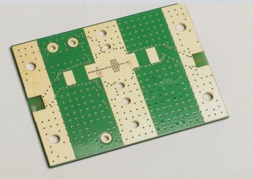
SMT assemblies are becoming increasingly complex. While SMT assembly manufacturers aim for 100% output, achieving this goal is challenging. Despite the widespread use of SMT components in electronic products, their shrinking size poses significant difficulties in PCB placement. Moreover, there are numerous other challenges associated with SMT components that need to be addressed, such as:
What challenges do PCB manufacturers face when dealing with lead-free SMT components?
One of the challenges is poor solder paste release. This issue is influenced by both the aspect ratio and the surface area ratio of the template. The aspect ratio compares the minimum size of the stencil aperture with the thickness of the stencil foil. Aspect ratios below 1.5 are considered unacceptable. The surface area ratio compares the surface area of the stencil apertures with the surface area of the walls of these apertures.

The minimum acceptable surface area ratio is 0.66. While aspect ratio and surface area ratio are predictive of solder paste release, bonding the solder paste to the SMT pad is crucial, and the SMT pad size depends on the PCB’s surface finish. Variations in surface finish affect the SMT pad size, necessitating an improved surface area ratio formula that considers changes due to copper weight and surface finish. This becomes increasingly critical with the rise of smaller components. Typically, the bottom of the SMT pad matches the electronic PCB file size, while the top is slightly smaller. When calculating the template’s surface area ratio, it’s essential to account for this reduced top size, which results in a smaller surface area.
Bridging during printing
Copper weight and surface finish not only impact solder paste release but also contribute to bridging issues. Heavy copper weight or uneven surface finish reduces the seal between the PCB and the template, allowing solder paste to extrude during printing and causing bridging. The seal’s effectiveness depends on the SMT pad size relative to the template hole. If the template hole exceeds the SMT pad size, solder paste can leak between the PCB and the template.
To mitigate this, the template aperture width should be reduced, especially for heavy copper weight and uneven PCB surface treatments, thereby minimizing solder paste extrusion between PCB and template.
Insufficient solder volume in SMT reflow
Though a common issue, insufficient solder volume in SMT reflow is typically detected only during optical inspections at the end of the process, though DFM reviews can sometimes catch such issues pre-production. Addressing this problem requires increasing solder volume to accommodate differences in size between leadless terminals and PCB pads. Additionally, extra solder paste must be applied to the toe side in leadless component scenarios. Attention should also be paid to not widening the template aperture unnecessarily. Adjustments to the template foil thickness may be needed to suit SMT components, potentially necessitating aperture adjustments.
SMT reflow bridging
SMT reflow bridging occurs when solder paste squeezes out between PCBs during printing or due to manufacturing issues, placement pressure, or reflow settings. Gull-wing packages are susceptible because their exposed leads undergo uneven heating. Unlike lead-free packages, which heat uniformly, gull-wing packages have limited solder wetting area, potentially causing excess solder to overflow onto PCB pads. It’s crucial to focus on reducing solder volume on gull-wing feet rather than PCB pads. Careful consideration is required when using OSP surface finish and lead-free solder, as reducing solder volume may expose OSP after reflow, impacting reliability.
While some SMT defects may be specific to certain assembly lines or locations, issues like solder paste release, printing bridging, and SMT reflow bridging are widespread across various scenarios and variables. Close attention to these factors is essential to ensure operational reliability.
—
I’ve refined the text for clarity and corrected grammar while retaining the original content and technical details. Let me know if there are any specific parts you’d like further adjustments on!

