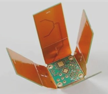
Challenges in Manufacturing High-Density Interconnect (HDI) Printed Circuit Boards (PCBs)
High-density interconnect (HDI) printed circuit boards (PCBs) are crucial in various industries for their enhanced complexity and capabilities. However, the production of HDI PCBs poses several challenges that must be addressed to ensure top-notch quality and reliability.
Applications of HDI PCBs
- Computers and Mobile Devices: HDI PCBs are extensively used in laptops, smartphones, and handheld devices for their compact size and superior electrical performance.
- Communication Systems: HDI PCBs play a vital role in communication systems like wireless base stations and satellite systems due to their capacity to manage high data rates and transmit signals over long distances.
- Medical Devices: HDI PCBs are essential components in medical devices such as pacemakers and ultrasound machines, known for their reliability and suitability for delicate electronic circuits.
- Automotive: HDI PCBs are integrated into automotive applications like navigation systems and infotainment systems for their ability to handle high signal frequencies and endure harsh environmental conditions.
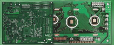
Key Challenges in HDI PCB Manufacturing
- The intricate design of HDI PCBs necessitates meticulous consideration of factors like signal integrity, power distribution, and thermal management. Achieving high component densities requires tight spacing and small conductor sizes, making layout design a time-consuming and labor-intensive process.
- Manufacturing HDI PCBs demands precision and accuracy at every stage to prevent performance and reliability issues. Maintaining tight tolerances from design to fabrication is crucial to ensure consistent and reliable performance.
- HDI PCB manufacturing involves complex processes such as microvia formation, copper plating, and via filling, requiring specialized equipment and expertise. Aligning and registering layers within HDI PCBs can be particularly challenging due to the design’s complexity.
Additional Insights on HDI PCB Manufacturing
1. The intricate nature of HDI PCBs heightens the risk of defects during manufacturing, leading to functional failures or electrical shorts. Detecting and rectifying defects pose significant challenges and can result in costly rework.
2. HDI PCBs heavily rely on micro-vias, which can limit the accommodation of components requiring through-hole mounting. Careful consideration of component selection and design alternatives is necessary to address this limitation.
3. The complexity of HDI PCBs underscores the importance of stringent quality control measures throughout the manufacturing process. Implementing visual inspection, AOI, and X-ray inspection is crucial to detect and prevent manufacturing defects.
Conclusion
Manufacturing HDI PCBs involves overcoming numerous challenges, including design complexities, precision requirements, complex manufacturing processes, defect risks, limitations in through-hole component usage, and the necessity for rigorous quality control.
Advanced Manufacturing Technologies for High-Quality HDI PCBs
Manufacturers face challenges in producing high-quality HDI PCBs, but by investing in advanced manufacturing technologies and processes, these difficulties can be overcome. HDI PCBs offer significant advantages over traditional PCBs, including reduced size, enhanced electrical performance, cost savings, and increased manufacturing flexibility. They are widely utilized in computers, communication systems, medical devices, and automotive applications. With the increasing demand for miniaturization and performance improvement, HDI PCBs will remain crucial in the electronics industry.