At present, high-frequency and high-speed PCB design has become the norm, and every PCB layout engineer should be well-versed in this area. Next, Banermei will share some design insights from hardware experts in high-frequency and high-speed PCB circuits, hoping they will be beneficial to everyone.
1. How can we minimize high-frequency interference?
The fundamental approach to minimizing high-frequency interference is to reduce the electromagnetic field interference from high-frequency signals, commonly known as crosstalk. One effective strategy is to increase the distance between high-speed signals and analog signals or to add ground guard/shunt traces adjacent to the analog signals. Additionally, be mindful of noise interference between the digital ground and the analog ground.
2. How should impedance matching be considered when designing high-speed PCB schematics?

1. When designing high-speed PCB circuits, impedance matching is a critical design element. The impedance value is directly influenced by various factors, including the routing method (such as microstrip on the surface layer or stripline/double stripline in the inner layer), the distance from the reference layer (power or ground layer), trace width, and PCB material. These factors collectively affect the characteristic impedance of the trace. In essence, the impedance value can only be accurately determined after routing. Typically, simulation software may not account for certain routing conditions that involve discontinuous impedance due to limitations in the circuit model or mathematical algorithms used. In such cases, terminators (like series resistors) can be included in the schematic to mitigate the impact of impedance discontinuities. The best approach is to proactively avoid impedance discontinuities during the routing process.
2. In high-speed PCB design, what aspects should designers consider regarding EMC and EMI regulations?
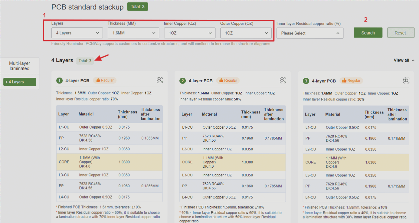
EMI/EMC design must address both radiated and conducted emissions simultaneously. Radiated emissions typically concern higher frequencies (<30MHz), while conducted emissions relate to lower frequencies (<30MHz). Therefore, it's essential not to focus solely on high frequencies while neglecting low frequencies. Effective EMI/EMC design requires consideration of device placement, PCB stack arrangement, critical connection methods, and device selection right from the layout stage. Without proper initial arrangements, resolving issues later can be significantly more challenging and costly. For instance, a clock generator should ideally be positioned away from external connectors, and high-speed signals should be routed to the inner layers whenever possible. It is crucial to ensure characteristic impedance matching and maintain continuity of the reference layer to minimize reflections. The slew rate of signals driven by devices should be kept as low as feasible to reduce high-frequency components. When selecting decoupling/bypass capacitors, verify that their frequency response meets the necessary requirements to minimize noise on the power plane. Additionally, consider the return path of high-frequency signal currents to keep the loop area (and thus loop impedance) small, thereby reducing radiation. Dividing the ground can also help control the extent of high-frequency noise. Finally, ensure proper grounding between the PCB and the chassis.
3. How should one choose a PCB board?
Selecting a PCB board requires balancing design requirements with mass production and cost considerations. Design requirements encompass both electrical and mechanical aspects. This material selection becomes especially critical when designing very high-speed PCBs (frequencies exceeding GHz). For instance, commonly used FR-4 material exhibits significant dielectric loss at GHz frequencies, which can greatly affect signal attenuation and may render it unsuitable. From an electrical perspective, it’s essential to assess whether the dielectric constant and dielectric loss align with the intended frequency.
4. How can one meet EMC requirements without imposing excessive cost pressures?
The increased costs associated with meeting EMC standards often arise from the need for additional ground layers to enhance shielding effectiveness and from incorporating components like ferrite beads and chokes for high-frequency harmonic suppression. Furthermore, it is generally necessary to align the shielding structure with other systems to ensure the entire setup meets EMC requirements.
1. How can we minimize high-frequency interference?
The fundamental approach to minimizing high-frequency interference is to reduce the electromagnetic field interference from high-frequency signals, commonly known as crosstalk. One effective strategy is to increase the distance between high-speed signals and analog signals or to add ground guard/shunt traces adjacent to the analog signals. Additionally, be mindful of noise interference between the digital ground and the analog ground.
2. How should impedance matching be considered when designing high-speed PCB schematics?

1. When designing high-speed PCB circuits, impedance matching is a critical design element. The impedance value is directly influenced by various factors, including the routing method (such as microstrip on the surface layer or stripline/double stripline in the inner layer), the distance from the reference layer (power or ground layer), trace width, and PCB material. These factors collectively affect the characteristic impedance of the trace. In essence, the impedance value can only be accurately determined after routing. Typically, simulation software may not account for certain routing conditions that involve discontinuous impedance due to limitations in the circuit model or mathematical algorithms used. In such cases, terminators (like series resistors) can be included in the schematic to mitigate the impact of impedance discontinuities. The best approach is to proactively avoid impedance discontinuities during the routing process.
2. In high-speed PCB design, what aspects should designers consider regarding EMC and EMI regulations?
EMI/EMC design must address both radiated and conducted emissions simultaneously. Radiated emissions typically concern higher frequencies (<30MHz), while conducted emissions relate to lower frequencies (<30MHz). Therefore, it's essential not to focus solely on high frequencies while neglecting low frequencies. Effective EMI/EMC design requires consideration of device placement, PCB stack arrangement, critical connection methods, and device selection right from the layout stage. Without proper initial arrangements, resolving issues later can be significantly more challenging and costly. For instance, a clock generator should ideally be positioned away from external connectors, and high-speed signals should be routed to the inner layers whenever possible. It is crucial to ensure characteristic impedance matching and maintain continuity of the reference layer to minimize reflections. The slew rate of signals driven by devices should be kept as low as feasible to reduce high-frequency components. When selecting decoupling/bypass capacitors, verify that their frequency response meets the necessary requirements to minimize noise on the power plane. Additionally, consider the return path of high-frequency signal currents to keep the loop area (and thus loop impedance) small, thereby reducing radiation. Dividing the ground can also help control the extent of high-frequency noise. Finally, ensure proper grounding between the PCB and the chassis.
3. How should one choose a PCB board?
Selecting a PCB board requires balancing design requirements with mass production and cost considerations. Design requirements encompass both electrical and mechanical aspects. This material selection becomes especially critical when designing very high-speed PCBs (frequencies exceeding GHz). For instance, commonly used FR-4 material exhibits significant dielectric loss at GHz frequencies, which can greatly affect signal attenuation and may render it unsuitable. From an electrical perspective, it’s essential to assess whether the dielectric constant and dielectric loss align with the intended frequency.
4. How can one meet EMC requirements without imposing excessive cost pressures?
The increased costs associated with meeting EMC standards often arise from the need for additional ground layers to enhance shielding effectiveness and from incorporating components like ferrite beads and chokes for high-frequency harmonic suppression. Furthermore, it is generally necessary to align the shielding structure with other systems to ensure the entire setup meets EMC requirements.


