Currently, high-frequency and high-speed PCB design has become the standard, and every PCB layout engineer should be well-versed in this area. Next, Banermei will share some design insights from hardware experts on high-frequency and high-speed PCB circuits, which we hope will be beneficial to all.
**What challenges might arise in high-frequency and high-speed PCB design?**
1. **How can we avoid high-frequency interference?**
The fundamental approach to minimizing high-frequency interference is to reduce the electromagnetic field disturbance caused by high-frequency signals, commonly referred to as crosstalk. One can increase the distance between high-speed and analog signals or incorporate ground guard/shunt traces adjacent to the analog signals. It’s also crucial to be mindful of noise interference from the digital ground to the analog ground.
2. **How should impedance matching be considered when designing high-speed PCB schematics?**
Impedance matching is a critical design factor in high-speed PCB circuits. The impedance value is inherently linked to the routing method, whether on the surface layer (microstrip) or inner layer (stripline/double stripline), the distance from the reference layer (power or ground layer), trace width, PCB material, and more. All these factors influence the characteristic impedance of the traces. Consequently, the impedance value can only be accurately defined post-routing. Typically, simulation software may not account for certain routing scenarios with discontinuous impedance due to limitations in circuit modeling or mathematical algorithms. In such cases, it’s advisable to include some termination elements, like series resistors, on the schematic to mitigate the effects of trace impedance discontinuities. Ultimately, the best solution is to avoid impedance discontinuities during the routing phase.
3. **In high-speed PCB design, what aspects should designers consider regarding EMC and EMI regulations?**
EMI/EMC design generally requires simultaneous consideration of both radiated and conducted aspects. The former pertains to higher frequency ranges (<30MHz), while the latter addresses lower frequency ranges (<30MHz). Therefore, it’s essential not to focus solely on high frequencies at the expense of low frequencies. Effective EMI/EMC design must take into account device placement, PCB stack configuration, critical connection methods, and device selection right from the layout’s inception. Failing to optimize these arrangements beforehand can lead to significant challenges later, resulting in increased costs and effort. For instance, the clock generator should not be positioned close to external connectors, and high-speed signals should ideally be routed to inner layers. It’s vital to maintain characteristic impedance matching and ensure continuity of the reference layer to minimize reflections. The signal slew rate should be kept as low as possible to reduce high-frequency components. When selecting decoupling/bypass capacitors, it’s important to verify that their frequency response meets the necessary requirements to minimize power plane noise. Additionally, attention should be given to the return path of high-frequency signal currents to keep the loop area as small as possible, thereby reducing radiation. Ground segmentation can also be employed to manage high-frequency noise effectively. Finally, appropriately selecting the chassis ground between the PCB and housing is crucial.
4. **How should one choose a PCB board?**
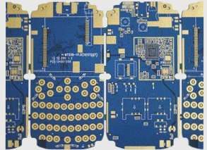
The choice of PCB materials must balance design requirements with mass production and cost considerations. Design requirements encompass both electrical and mechanical aspects. This material selection becomes particularly critical in the design of very high-speed PCBs (with frequencies exceeding GHz). For instance, the widely used FR-4 material exhibits significant dielectric loss at several GHz, impacting signal attenuation, and may not be suitable. From an electrical standpoint, it’s essential to ensure that the dielectric constant and dielectric loss are appropriate for the targeted frequency.
5. How can we meet EMC requirements while minimizing cost pressures?
The increased costs associated with PCB boards due to EMC considerations typically arise from the need for additional ground layers to enhance shielding and the inclusion of ferrite beads, chokes, and other high-frequency harmonic suppression devices. Moreover, it is often necessary to align the shielding structures with other components of the system to ensure compliance with EMC requirements. Below are several PCB design techniques aimed at reducing electromagnetic radiation generated by the circuit:
– Opt for devices with slower signal slew rates to minimize high-frequency components.
– Carefully place high-frequency components away from external connectors.
– Ensure proper impedance matching for high-speed signals, taking into account the routing layer and return current paths to reduce high-frequency reflections and radiation.
– Use adequate and appropriately rated decoupling capacitors on the power supply pins of each device to mitigate noise on both the power and ground planes. Special attention should be paid to ensure that the frequency response and temperature characteristics of the capacitors meet design specifications.
– Consider properly isolating the ground near the external connector, connecting the connector ground to the nearby chassis ground.
– Utilize ground guard/shunt traces beside certain high-speed signals as needed, but be mindful of their impact on the trace’s characteristic impedance.
– Position the power layer 20H away from the ground layer, where H represents the distance between the power and ground layers.
6. What factors should be considered when designing, routing, and laying out high-frequency PCBs above 2 GHz?
High-frequency PCBs above 2 GHz fall within the realm of radio frequency circuit design and extend beyond the traditional high-speed digital circuit design scope. The layout and routing of RF circuits must be considered in conjunction with the schematic, as these elements can produce distribution effects. Additionally, some passive components in RF circuit design are implemented using parameterized definitions and custom-shaped copper foils. Therefore, EDA tools need to support parameterized devices and custom copper foil editing. Mentor’s BoardStation features a specialized RF design module that meets these needs. Furthermore, effective RF design typically requires specialized RF circuit analysis tools, with Agilent’s EESoft being a notable industry leader, offering seamless integration with Mentor’s tools.
7. Do test points impact the quality of high-speed signals?
The effect of test points on signal quality largely depends on how they are incorporated and the speed of the signal. In general, additional test points (avoiding existing vias or DIP pins) can be added directly to the line or connected via a short branch. The former acts like a small capacitor added to the line, while the latter creates an additional branch. Both scenarios can influence high-speed signals to varying degrees, with the impact relating to the signal’s frequency and edge rate. This effect can be assessed through simulation. In principle, smaller test points are preferable (as long as they meet testing tool requirements), and shorter branches are advantageous.
If you have any PCB manufacturing needs, please do not hesitate to contact me.Contact me

