Difficulties in Making Inner Circuit
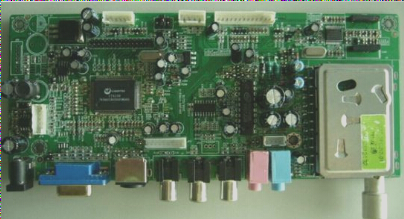
The multilayer circuit has various special requirements for high speed, thick copper, high frequency, and high Tg value. The requirements for inner layer wiring and pattern size control are becoming increasingly stringent. For example, the ARM development board contains numerous impedance signal lines in the inner layer. Ensuring the integrity of the impedance further complicates inner line production.
There are numerous signal lines in the inner layer, with line widths and spacing typically around 4mil or less. The thin production of multi-core boards is susceptible to wrinkles, which can increase difficulties in inner layer production.
Suggestion: Design the line width and spacing above 3.5/3.5mil (most factories can easily produce this).
For example, for a six-layer board, it is recommended to utilize a faux eight-layer structure design, which can meet impedance requirements of 50ohm, 90ohm, and 100ohm with line widths of 4-6mil in the inner layer.
Difficulties in Alignment Between Inner Layers
The number of multi-layer boards is on the rise, and the alignment requirements of the inner layers are becoming more stringent. Film expansion and contraction due to workshop temperature and humidity can affect alignment accuracy between layers, presenting challenges in control.
Difficulties in the Pressing Process
The superposition of multiple core plates and PP (cured plate) can lead to issues like delamination, slippage, and steam drum residue during pressing. In the structural design of the inner layer, factors such as dielectric thickness between layers, glue flow, and sheet heat resistance should be taken into account, and a well-designed laminated structure should be implemented.
Recommendation: Ensure even distribution of copper on the inner layer, spreading it over a large area without creating imbalance with PAD.
Difficulties in Drilling Production
The use of high Tg or other special plates in multi-layer boards results in varying drilling roughness for different materials, making slag removal more challenging. High-density multi-layer boards with high hole density can lead to low production efficiency and increased risk of breakage. Close proximity of via hole edges from different networks can cause CAF effect problems.
Suggestion: Maintain a hole edge spacing of ≥0.3mm between different networks.
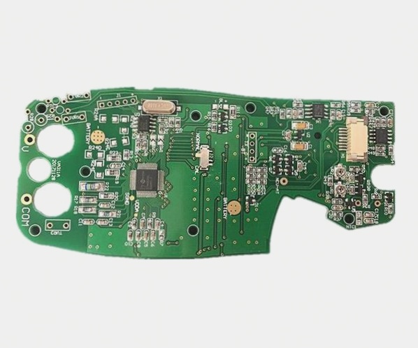
Multi-layer PCBs play a crucial role in various industries such as communications, healthcare, industrial control, security, automotive, electrical power, aviation, defense, and computer peripherals. As product capabilities continue to advance, the complexity of PCBs also increases, leading to greater challenges in production.


