Challenges in Multi-layer PCB Production
Multi-layer PCBs are essential in industries like communications, healthcare, and automotive. As technology advances, the complexity of PCBs increases, posing challenges in production.

Inner Circuit Challenges
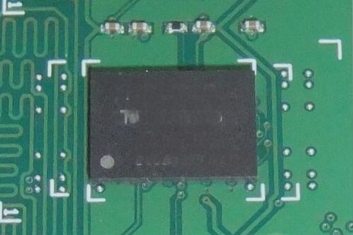
Creating multilayer circuits with high speed, thick copper, and high-frequency requirements presents difficulties in inner layer wiring and pattern control. Maintaining impedance integrity in the inner layer production is crucial, especially with numerous signal lines and small line widths.

Solution: Optimal Design
Designing with line widths and spacing above 3.5/3.5mil can simplify production. Utilizing a faux eight-layer design for a six-layer board can meet impedance requirements effectively.
Alignment Between Layers
With the increasing number of multi-layer boards, precise alignment between inner layers becomes more challenging due to factors like temperature and humidity affecting film expansion and contraction.
Pressing Process Issues
Problems like delamination and slippage can occur during the pressing process of multi-core boards. A well-designed laminated structure and even copper distribution on the inner layers are crucial to prevent these issues.
Drilling Production Difficulties
Using special plates in multi-layer boards can lead to varying drilling roughness, making slag removal tough. Maintaining proper hole edge spacing between different networks is essential to avoid production inefficiencies and CAF effect problems.