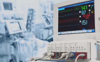
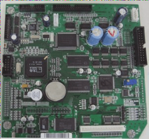
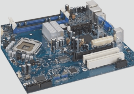
1. In short, printed circuit boards (PCBs) are essential for the proper functioning of all electronic devices. Therefore, when there is an issue with a PCB, electronic equipment may not perform as expected. PCB-related problems pose a significant challenge for manufacturers, as numerous issues can arise, particularly during the multi-layer PCB manufacturing process. Below are seven common problems encountered in the manufacturing of multi-layer PCBs.
2. By understanding these issues, designers can address them during the PCB design phase, aiming to prevent potential damage to the printed circuit board.
3. Design: During the design of multi-layer PCBs, issues related to bowing and twisting can occur. Bowing and twisting are key factors used to assess PCB flatness. Bowing refers to cylindrical or spherical curvature, while twisting involves deformation parallel to the PCB’s diagonal.
4. To ensure the production of high-quality multi-layer PCBs, service providers should follow several steps. Fortunately, many PCB manufacturing companies implement practices to minimize bowing and twisting. First, manufacturers should use appropriate parameters when pressing multi-layer PCBs to reduce stress on the board. Second, they should avoid mixing materials from different suppliers. Third, all materials should comply with RoHS guidelines. Additionally, PCB manufacturers should use or adopt horizontal ovens during the curing process to prevent issues related to PCB bowing and twisting.
5. Press multi-layer PCB

1. Multilayer printed circuit boards (PCBs) consist of multiple single-layer boards that need to be stacked together. Laminate involves laying out the insulating and copper layers before the PCB layout design to create a printed circuit board.
2. In manufacturing multilayer printed circuit boards, challenges arise in laminating the insulating and copper layers together. Many manufacturers often face difficulties during the pressing process of the multilayer PCB components.
3. To ensure a smooth stacking process for multilayer printed circuit boards, manufacturers should not only use high-quality laminate materials but also select the most appropriate machinery for the task.
4. **The Choice of Substrate**
5. PCB materials serve two fundamental purposes: conducting electricity and providing insulation between conductive copper layers. Therefore, choosing the right substrate material is crucial to the success or failure of a printed circuit board. It also impacts the PCB’s thermal behavior, mechanical properties, and electrical characteristics.
6. **Dielectric Constant**
7. Since the functions of most printed circuit boards are determined by the substrate material, high-frequency substrates are required for high-speed and high-frequency PCBs. These substrates must have a low and stable dielectric constant.
8. **Substrate Characteristics**
9. Additionally, the substrate material must exhibit good heat resistance, stability, impact strength, chemical resistance, and manufacturability. For high-speed and high-frequency PCBs, substrate materials should have low moisture absorption or be composed of low moisture-absorbing materials. Copper foil also needs to provide high peel strength.
10. **Insulation**
11. FR4, also known as FR-4, is one of the most versatile and cost-effective multilayer substrate materials, offering excellent performance. FR-4 provides superior electrical insulation with high dielectric strength.
12. **Multilayer PCB Manufacturing—Resin Penetration**
13. The resin plugging process is a standard procedure in the printed circuit board industry, especially for high-frequency products requiring substantial thickness and high-layer counts. Recently, resin plugging technology has become increasingly widespread, particularly in HDI panels. For issues that cannot be resolved by pressure filling or green oil plugging resin, using resin for plugging is recommended.
14. Resin plugging is a common challenge in multilayer PCB manufacturing. The optimal solution is to use a vacuum plug machine.
15. Resin plugging serves as a preventive measure to protect through holes from accidental solder flow, particularly during soldering and assembly. Its primary function is to secure fibers and shield them from external factors.
16. **Dense Heat Dissipation Hole Manufacturing**
17. Heat dissipation is crucial in PCB manufacturing. It involves transferring heat from hotter objects to cooler environments, which occurs through convection, conduction, and radiation.
18. Many PCB manufacturers face challenges related to heat dissipation. To address intensive heat dissipation issues, using recommended heat dissipation materials, such as aluminum, is advisable.
19. **Multilayer PCB Manufacturing—Back Drill Production**
20. Back drilling is an effective technique used in high-speed multilayer printed circuit boards to minimize parasitic effects of plated through holes. Also known as controlled-depth drilling, this method removes unused parts, stubs, and copper pipes from the through holes on the PCB.
21. Back drilling improves signal integrity and reduces manufacturing difficulties while also decreasing noise interference. However, it presents challenges, such as hole cleaning, barite depressions, stuck tubes, circulation losses, and shale instability.
22. **Multilayer PCB Manufacturing—Testing**
23. Testing is an essential phase in the PCB development cycle. In the PCB manufacturing process, testing can help save costs and prevent issues or complications in the final production run.
24. Unfortunately, many PCB manufacturing companies encounter failures in multilayer manufacturing when employing testing methods. Recommended testing methods include bare board testing, in-circuit testing, functional testing, and assembly-level testing. Effective testing can identify technical defects in multilayer printed circuit boards.
2. By understanding these issues, designers can address them during the PCB design phase, aiming to prevent potential damage to the printed circuit board.
3. Design: During the design of multi-layer PCBs, issues related to bowing and twisting can occur. Bowing and twisting are key factors used to assess PCB flatness. Bowing refers to cylindrical or spherical curvature, while twisting involves deformation parallel to the PCB’s diagonal.
4. To ensure the production of high-quality multi-layer PCBs, service providers should follow several steps. Fortunately, many PCB manufacturing companies implement practices to minimize bowing and twisting. First, manufacturers should use appropriate parameters when pressing multi-layer PCBs to reduce stress on the board. Second, they should avoid mixing materials from different suppliers. Third, all materials should comply with RoHS guidelines. Additionally, PCB manufacturers should use or adopt horizontal ovens during the curing process to prevent issues related to PCB bowing and twisting.
5. Press multi-layer PCB
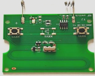
1. Multilayer printed circuit boards (PCBs) consist of multiple single-layer boards that need to be stacked together. Laminate involves laying out the insulating and copper layers before the PCB layout design to create a printed circuit board.
2. In manufacturing multilayer printed circuit boards, challenges arise in laminating the insulating and copper layers together. Many manufacturers often face difficulties during the pressing process of the multilayer PCB components.
3. To ensure a smooth stacking process for multilayer printed circuit boards, manufacturers should not only use high-quality laminate materials but also select the most appropriate machinery for the task.
4. **The Choice of Substrate**
5. PCB materials serve two fundamental purposes: conducting electricity and providing insulation between conductive copper layers. Therefore, choosing the right substrate material is crucial to the success or failure of a printed circuit board. It also impacts the PCB’s thermal behavior, mechanical properties, and electrical characteristics.
6. **Dielectric Constant**
7. Since the functions of most printed circuit boards are determined by the substrate material, high-frequency substrates are required for high-speed and high-frequency PCBs. These substrates must have a low and stable dielectric constant.
8. **Substrate Characteristics**
9. Additionally, the substrate material must exhibit good heat resistance, stability, impact strength, chemical resistance, and manufacturability. For high-speed and high-frequency PCBs, substrate materials should have low moisture absorption or be composed of low moisture-absorbing materials. Copper foil also needs to provide high peel strength.
10. **Insulation**
11. FR4, also known as FR-4, is one of the most versatile and cost-effective multilayer substrate materials, offering excellent performance. FR-4 provides superior electrical insulation with high dielectric strength.
12. **Multilayer PCB Manufacturing—Resin Penetration**
13. The resin plugging process is a standard procedure in the printed circuit board industry, especially for high-frequency products requiring substantial thickness and high-layer counts. Recently, resin plugging technology has become increasingly widespread, particularly in HDI panels. For issues that cannot be resolved by pressure filling or green oil plugging resin, using resin for plugging is recommended.
14. Resin plugging is a common challenge in multilayer PCB manufacturing. The optimal solution is to use a vacuum plug machine.
15. Resin plugging serves as a preventive measure to protect through holes from accidental solder flow, particularly during soldering and assembly. Its primary function is to secure fibers and shield them from external factors.
16. **Dense Heat Dissipation Hole Manufacturing**
17. Heat dissipation is crucial in PCB manufacturing. It involves transferring heat from hotter objects to cooler environments, which occurs through convection, conduction, and radiation.
18. Many PCB manufacturers face challenges related to heat dissipation. To address intensive heat dissipation issues, using recommended heat dissipation materials, such as aluminum, is advisable.
19. **Multilayer PCB Manufacturing—Back Drill Production**
20. Back drilling is an effective technique used in high-speed multilayer printed circuit boards to minimize parasitic effects of plated through holes. Also known as controlled-depth drilling, this method removes unused parts, stubs, and copper pipes from the through holes on the PCB.
21. Back drilling improves signal integrity and reduces manufacturing difficulties while also decreasing noise interference. However, it presents challenges, such as hole cleaning, barite depressions, stuck tubes, circulation losses, and shale instability.
22. **Multilayer PCB Manufacturing—Testing**
23. Testing is an essential phase in the PCB development cycle. In the PCB manufacturing process, testing can help save costs and prevent issues or complications in the final production run.
24. Unfortunately, many PCB manufacturing companies encounter failures in multilayer manufacturing when employing testing methods. Recommended testing methods include bare board testing, in-circuit testing, functional testing, and assembly-level testing. Effective testing can identify technical defects in multilayer printed circuit boards.

