Latest Trends in PCB Manufacturing
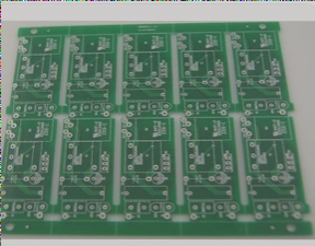
1. Shrinking PCB Circuits and Increasing Layers
With the continuous advancement of the electronics industry, PCB manufacturers are integrating electronic components more tightly, leading to a significant reduction in size. Ball Grid Array (BGA) packages have become the standard choice, resulting in smaller PCB circuits with an increased number of layers. To maximize limited space, line width and spacing are being reduced, and the number of layers is being increased. In the future, main signal traces on circuit boards are expected to be as small as 2-3 mils or even smaller.
2. Balancing Investment and Production Upgrades
Upgrading the production process to a higher grade requires a substantial investment, especially for high-end circuit boards produced using advanced equipment. Not all companies can afford such investments, and conducting trial production after such upgrades can be time-consuming and costly. A practical approach involves experimenting and conducting trial runs based on current capabilities before deciding on further investments based on results and market conditions.
3. PCB Production Methods
The production process for PCBs typically involves two main methods: the cover-hole acid etching method and the pattern electroplating method. Each method has its advantages and disadvantages, with considerations for circuit uniformity, environmental impact, and quality control.
4. Importance of Dry Film in PCB Production
Dry film is crucial in PCB production, with different types offering varying resolution capabilities. Standard exposure machines can achieve resolutions of 2 mils, making line width and spacing issues generally manageable. Development machines working with smaller line widths require careful consideration of pressure, concentration, and nozzle shape for optimal resolution.
5. Impact of Exposure Energy and Developing Conditions
Exposure energy significantly impacts circuit quality, with available dry films offering a wide exposure range. Developing conditions become more critical as line widths decrease, with factors such as speed, solution concentration, pressure, and nozzle shape affecting resolution. Proper development is crucial for achieving fine lines and optimal circuit appearance.
Different Exposure Machines and Etching Techniques in PCB Production
- Exposure machines vary in resolution capabilities, with air-cooled and water-cooled options commonly used.
- Special adjustments can achieve resolutions finer than the nominal rating of 4mil, such as 0.2mil, but caution is needed to prevent dust and debris interference.
- The “mushroom effect” in alkaline etching can be mitigated by techniques like pulse electroplating and using thicker dry films.
- Thin line film removal challenges can be addressed by adjusting lead and tin plating thickness and sodium hydroxide concentration.
- Etching speed in alkaline etching depends on line width and shape, with specific considerations for copper foil thickness and nozzle type.
- Acid etching offers better line definition compared to alkaline etching, with fan-shaped nozzles providing superior results.
- Factors like film speed, temperature, and cleanliness significantly impact PCB production yield rates.
- Standard equipment can produce 3.0mil circuits, but environmental factors and operator skill levels influence yield rates.
If you have any questions about PCB production, please contact info@wellcircuits.com.