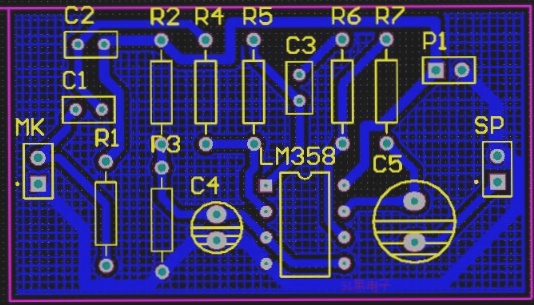
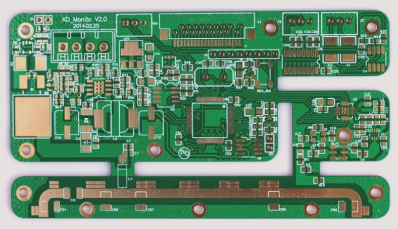
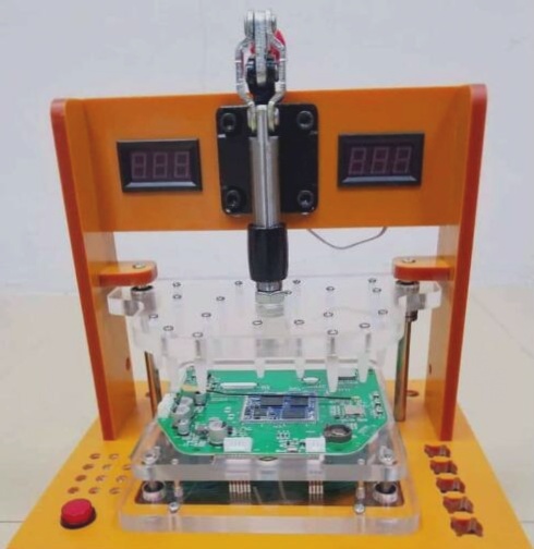
The quality of PCB circuit boards is generally assessed by appearance, though this often relies on experience. The quality of PCB circuit boards is crucial. So, what are the characteristics of high-quality PCB circuit boards?
1. **25-micron hole wall copper thickness**
**Benefits:** Enhances reliability, including improving the z-axis expansion resistance.
**Risks of not doing this:** Potential blow holes or degassing, electrical connectivity issues during assembly (inner layer separation, hole wall breakage), or failure under load conditions in actual use. IPC Class 2 (the standard adopted by most PCB factories) permits 20% less copper plating.
2. **No welding repairs or open circuit repairs**
**Benefits:** A perfect circuit ensures reliability and safety, with no need for maintenance and no associated risks.
**Risks of not doing this:** Improper repairs can lead to circuit board failure. Even if repairs are made ‘properly,’ there remains a risk of failure under load conditions (e.g., vibration), which may cause problems in actual use.
3. **Strictly controlling the service life of each surface treatment**
**Benefits:** Enhances solderability, reliability, and reduces the risk of moisture intrusion.
**Risks of not doing this:**

1. Due to metallographic changes in the surface treatment of old circuit boards, soldering issues may arise, and moisture intrusion can lead to problems such as delamination, separation (open circuit) of the inner layer, and the hole wall during assembly and/or use.
2. The tolerance of the copper-clad laminate meets IPC-4101 Class B/L requirements.
Benefits: Strict control of dielectric layer thickness helps reduce deviations in expected electrical performance.
The risk of not doing so: Electrical performance may not meet specifications, leading to significant performance variations within the same batch.
3. Define solder mask materials to ensure compliance with IPC-SM-840 Class T requirements.
Benefits: “Excellent” ink ensures safety and that solder mask ink meets UL standards.
The risk of not doing so: Inferior inks can cause issues with adhesion, flux resistance, and hardness, leading to solder mask separation and potential copper circuit corrosion. Poor insulation can result in short circuits due to accidental electrical continuity or arcs.
4. Defining tolerances for shapes, holes, and other mechanical features.
Benefits: Strict control of tolerances enhances product dimensional quality, improving fit, shape, and function.
The risk of not doing so: Assembly issues may arise, such as misalignment or fit problems, often discovered only after assembly. Increased size deviation can also cause installation issues.
5. Requirements for solder mask thickness, despite IPC not having specific regulations.
Benefits: Improved electrical insulation, reduced risk of peeling or loss of adhesion, and enhanced resistance to mechanical impact regardless of the impact location.
The risk of not doing so: Thin solder masks can lead to adhesion, flux resistance, and hardness issues, resulting in solder mask separation and potential copper circuit corrosion. Poor insulation from a thin solder mask can also cause short circuits due to accidental conduction or arcs.
1. **25-micron hole wall copper thickness**
**Benefits:** Enhances reliability, including improving the z-axis expansion resistance.
**Risks of not doing this:** Potential blow holes or degassing, electrical connectivity issues during assembly (inner layer separation, hole wall breakage), or failure under load conditions in actual use. IPC Class 2 (the standard adopted by most PCB factories) permits 20% less copper plating.
2. **No welding repairs or open circuit repairs**
**Benefits:** A perfect circuit ensures reliability and safety, with no need for maintenance and no associated risks.
**Risks of not doing this:** Improper repairs can lead to circuit board failure. Even if repairs are made ‘properly,’ there remains a risk of failure under load conditions (e.g., vibration), which may cause problems in actual use.
3. **Strictly controlling the service life of each surface treatment**
**Benefits:** Enhances solderability, reliability, and reduces the risk of moisture intrusion.
**Risks of not doing this:**

1. Due to metallographic changes in the surface treatment of old circuit boards, soldering issues may arise, and moisture intrusion can lead to problems such as delamination, separation (open circuit) of the inner layer, and the hole wall during assembly and/or use.
2. The tolerance of the copper-clad laminate meets IPC-4101 Class B/L requirements.
Benefits: Strict control of dielectric layer thickness helps reduce deviations in expected electrical performance.
The risk of not doing so: Electrical performance may not meet specifications, leading to significant performance variations within the same batch.
3. Define solder mask materials to ensure compliance with IPC-SM-840 Class T requirements.
Benefits: “Excellent” ink ensures safety and that solder mask ink meets UL standards.
The risk of not doing so: Inferior inks can cause issues with adhesion, flux resistance, and hardness, leading to solder mask separation and potential copper circuit corrosion. Poor insulation can result in short circuits due to accidental electrical continuity or arcs.
4. Defining tolerances for shapes, holes, and other mechanical features.
Benefits: Strict control of tolerances enhances product dimensional quality, improving fit, shape, and function.
The risk of not doing so: Assembly issues may arise, such as misalignment or fit problems, often discovered only after assembly. Increased size deviation can also cause installation issues.
5. Requirements for solder mask thickness, despite IPC not having specific regulations.
Benefits: Improved electrical insulation, reduced risk of peeling or loss of adhesion, and enhanced resistance to mechanical impact regardless of the impact location.
The risk of not doing so: Thin solder masks can lead to adhesion, flux resistance, and hardness issues, resulting in solder mask separation and potential copper circuit corrosion. Poor insulation from a thin solder mask can also cause short circuits due to accidental conduction or arcs.


