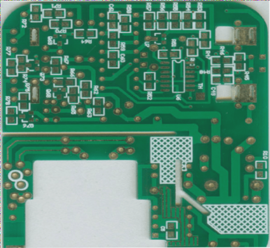
Why is Copper Essential in PCBs?
Copper plays a crucial role in PCBs for various reasons:
- EMC (Electromagnetic Compatibility): Large-area copper serves as a shielding mechanism, while specific ground planes offer protection.
- PCB Process Requirements: Copper is added to PCB layers to ensure proper electroplating and prevent deformation during lamination.
- Signal Integrity: Copper provides a return path for high-frequency digital signals, reducing interference and simplifying routing.
Advantages of Copper in PCBs
One key benefit of copper paving is the reduction of ground wire impedance, crucial for minimizing interference in digital circuits. It also aids in heat dissipation and device mounting. When laying circuit copper:
- Laying copper and connecting it to the ground wire reduces loop area.
- A large copper area lowers ground wire resistance and voltage drop.
FPC Board Structures
FPC boards are classified based on substrate material and structure:
1. Single-layer Soft Board Structure (FPC)
This basic FPC type consists of base material, transparent adhesive, and copper foil. The copper foil is etched to form circuits, and pads are exposed through drilling. The final product is a flexible slab with stamped circuit boards.
2. Double-layer Soft Board Structure (FPC)
Used for complex circuits, this structure involves adding vias to connect copper foil layers. Vias are created by drilling holes and plating copper, similar to single-layer boards.
3. Double-sided Soft Board Structure (FPC)
The Advantages of FPC Double-Sided Soft Boards
- Interconnecting with other circuit boards
- Utilizes copper foil, protective film, and transparent adhesive
- Unique manufacturing process
FPC double-sided soft boards are designed with pads on both sides, making them ideal for interconnecting with other circuit boards. While similar to single-layer boards, the manufacturing process differs significantly. The boards are crafted using copper foil, protective film, and transparent adhesive. Initially, holes are drilled into the protective film at the necessary pad locations. Subsequently, copper foil is applied, and the pads and leads are etched. Finally, an additional protective film layer with drilled holes is affixed to complete the structure.