PCB Board Plugging Holes: Enhancing Manufacturing Quality
Conductive holes, known as vias, are vital in printed circuit boards (PCBs) as they connect different layers. To meet customer specifications and ensure functionality, vias often need to be plugged. A modern method using white mesh material for PCB surface soldering and via plugging has emerged, enhancing production stability and quality.
Improving Processes with White Mesh
Transitioning from traditional aluminum to white mesh for via plugging on PCB surfaces has significantly improved efficiency and consistency in production. This innovation reduces defects, enhances reliability, and meets the stringent requirements of modern PCB designs.
Advantages of White Mesh Plugging
- Enhanced Stability: White mesh plugging offers better control, reducing errors and defects.
- Reliability: Ensures a stronger bond and improved mechanical properties for a more durable PCB.
- Cost-Efficiency: Cost savings in materials and labor without compromising quality.
Evolution of Plug Hole Technology
Via holes are crucial interconnections in PCBs for electrical lines. Advancements in surface mount technology have led to plug hole technology, ensuring functionality and reliability through specific requirements:
- Copper Presence: Vias must contain copper for reliable electrical conductivity, with solder mask plugging based on design needs.
- Tin-Lead Coating: Coated with tin-lead to a specific thickness to prevent solder mask ink interference.
- Solder Mask Plugging: Opaque solder mask prevents irregularities, ensuring clean connections during wave soldering.
Advantages of Plug Hole Technology
- Short Circuit Prevention: Plugged vias prevent solder flow, crucial for preventing short circuits, especially on pads.
- Flux Residue Prevention: Ensures flux residues do not affect circuit integrity.
- Vacuum Testing Integrity: Maintains negative pressure for proper testing after assembly.
- Solder Paste Containment: Prevents solder paste from affecting solder joints and placement.
- Wave Soldering Reliability: Ensures no solder ball formation, maintaining circuit functionality.
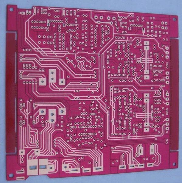
Key Components of a PCB
- Pads: Metalized holes for component pin soldering.
- Vias: Metalized holes linking component pins across layers.
- Mounting Holes: Used for physical PCB securing.
- Wires (Traces): Copper conductors establishing electrical connections.
- Connectors: Facilitate communication between PCBs.
PCB Layer Types and Technological Innovations
- Filling: Ground plane copper filling reduces impedance and enhances signal integrity.
- Electrical Boundaries: Define the PCB’s size and ensure that components remain within designated areas.
Common PCB Layer Configurations:
- Single-Layer PCB: Simplest design with one layer of conductive material.
- Double-Layer PCB: Contains conductive layers on both sides for more complex designs.
- Multilayer PCB: Offers multiple conductive layers for increased functionality and compactness in intricate designs.
The development of plug hole technology in PCBs reflects the growing need for precise and reliable manufacturing processes, supporting the continuous advancement of electronic devices. Technological innovations ensure that PCBs can meet higher performance standards while maintaining design flexibility.
Single-Layer Board
A single-layer PCB has copper on one side, with components mounted on the non-copper side. It is cost-effective and suitable for low-density applications but may be limited in more advanced uses.
Double-Layer Board
Double-layer PCBs have copper on both sides, offering increased flexibility for routing and component placement. Widely used in applications like power supplies and communication devices.
Multi-Layer Board
Multi-layer PCBs consist of several layers of copper and insulating material, providing improved performance and design density. Commonly used in high-performance electronics like smartphones and medical devices.