The Importance of Welding Gap in Welded Joints
The welding gap, also known as the butt gap, is the crucial space between two welded components at the butt joint. The size of this gap significantly influences the quality of the welded joint.

- When the welding gap is too small, penetration of the weld seam becomes challenging.
- Conversely, a gap that is too large poses difficulties in welding due to the excess filler material, impacting the welding process, increasing welding stress, and potentially causing deformation.
For optimum results, a spacing of 30-40 millimeters is generally recommended. The distance between welding points should align with the specifications of the welded part, striking a balance between density and sparsity.
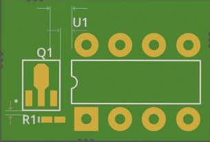
Spacing Considerations in PCB Design
- Spacing between wires: The distance between wires should not be less than 4 mils, with a minimum conventional value of 10 mils.
- Pad aperture and width: The minimum aperture for mechanically drilled solder mask apertures should be at least 0.2mm, while laser-drilled apertures are recommended to have a minimum of 4 mils. Aperture tolerance typically falls within 0.05mm. The welding pad’s minimum width should be no less than 0.2mm.
- Spacing between pads: Pads should maintain a spacing of no less than 0.2mm.
- Distance between copper layer and board edge: Ideally, the distance between the copper layer and the PCB edge should be no less than 0.3mm. For extensive copper areas, a typical inward shrink distance from the board edge is 20 mils.
- Distance from silkscreen to solder mask: Silkscreen should not overlap the solder pad to ensure proper tinning during soldering and component installation. An 8 mil spacing is generally recommended, with a 4 mil spacing being acceptable in compact PCB areas.
When designing a silkscreen frame, maintain a slight distance of about 6 mils from the solder pad to meet production and installation requirements. Any accidental overlap of silkscreen on the solder mask will be removed during manufacturing to facilitate smooth PCB board and SMT chip assembly.


