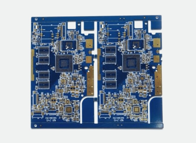
The process of copper coating entails using the unused space on the PCB as a reference plane and filling it with solid copper, also known as copper pouring. The primary aim of copper coating is to decrease the impedance of the ground wire and enhance anti-interference capabilities. Additionally, it reduces voltage drop, improves power supply efficiency, and reduces loop area when connected to the ground wire. When dealing with multiple grounds on the PCB, such as SGND, AGND, GND, etc., the approach is to pour copper independently based on the different positions of the PCB surface, using the main “ground” as a reference. It is important to separate digital ground and analog ground with copper. Prior to pouring copper, appropriate power connections should be thickened, such as V5.0V, V3.6V, V3.3V (SD card power supply), etc., to create multiple deformable structures of different shapes.
Several issues need to be addressed when it comes to copper coating, including single-point connection in different locations and copper coating near the crystal oscillator. The crystal oscillator is a high-frequency emission source, so it is surrounded by copper and the crystal oscillator shell ground is separated. Additionally, handling the island (dead zone) problem may involve defining a ground via and adding it. When it comes to the choice between large-area copper cladding and grid copper cladding, it’s not easy to make a generalization. Large-area copper may cause warping or blistering during wave soldering, so grid copper cladding is often preferred for its better heat dissipation.
In digital circuits, particularly those with high operating frequencies, copper coating serves to reduce the impedance of the entire ground plane. As for a specific processing method, each core module and all digital circuits will be partitioned with copper if possible, and then connected with wires to minimize circuit interference at all levels. When it comes to mixed circuits of digital and analog circuits, independent wiring of the ground wire and a summary to the power supply filter capacitor are crucial. However, it’s important to note that the ground wire distribution in analog circuits cannot simply be covered with a piece of copper, as the mutual influence of the front and rear stages is a key consideration. The analog ground requires a single point grounding and must be handled based on the specific situation.


