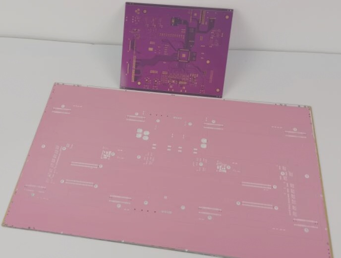
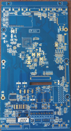
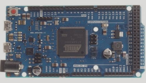
Copper Pour Techniques for PCB Design
Copper pour is a widely used method in PCB design to cover empty spaces on the board with a layer of copper film, enhancing the board’s resistance to interference. By filling unused areas with solid copper, known as copper fills, various benefits can be achieved:
- Lower ground impedance
- Improved interference resistance
- Reduced voltage drop
- Enhanced power supply efficiency
- Minimized loop areas
Considerations for Copper Pouring
- Single-point connection of different grounds using 0-ohm resistors, ferrite beads, or inductors
- Copper-cladding near the crystal oscillator to reduce high-frequency noise
- Addressing the island (dead zone) problem by defining ground vias
Benefits of Copper Coating
Copper coating can improve power efficiency, reduce high-frequency interference, and enhance the overall appearance of the PCB.
Choosing Between Large-Area and Grid Copper Pour
The decision between large-area and grid copper pour depends on the specific PCB requirements. While grid copper is ideal for high-frequency boards, full copper pours are suitable for low-frequency circuits with high current needs.
Precautions for Copper-Clad Wiring
When working with copper-clad PCBs, it is essential to set safety spacing correctly to avoid issues during the copper pouring process. Consider defining separate safety distance rules for copper pours to streamline the design process.
PCB Design Tips for Smooth Interaction Between Routing and Copper Pour Rules
- Update FullQuery Display: Change “IsPolygon” to “InPolygon” for better clarity.
- Adjust Copper Safety Gap: Ensure copper pours comply with routing safety spacing by adjusting the copper safety gap in the Constraints section.
Some designers argue that routing rules should take precedence over copper pour rules to maintain safety spacing. To address this, consider adding an exception for copper pours in the routing safety spacing rules within “FullQuery.” Alternatively, adjust priorities directly in the rule settings by increasing the priority of the copper-clad safety spacing rule. This adjustment will prioritize the copper-clad safety spacing over routing safety spacing, promoting a seamless interaction between both sets of rules.
PCB Copper-Clad Line Width Setting:
When utilizing “Hatched” or “None” modes, pay attention to the “TrackWidth” field. If the default 8 mil width is selected, and the minimum line width for the network connected to your copper pour exceeds 8 mil, a DRC error may occur. Ignoring this detail often results in multiple DRC errors post copper pour implementation.
If you require PCB manufacturing services or have any inquiries, feel free to contact me.