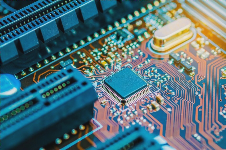
PCB warping, an industry term, refers to the bending of a flat PCB, also known as warping. In severe cases, this can resemble the arching of a bridge.
During actual production, PCBs are rarely perfectly flat and may exhibit some degree of bending. The degree of PCB warpage is typically assessed using “warpage.
According to IPC standards, PCBs intended for mounting should have a warpage of ≤ 0.75% to be considered qualified. Exceeding this threshold renders the PCB warped and thus unacceptable. For PCBs that do not require mounting (only containing plug-in components), the flatness requirement is less stringent, allowing for warpage up to ≤ 1.5%.
To meet the demands of high-precision and high-speed mounting, certain manufacturers impose stricter criteria for PCB warpage, setting limits as low as ≤ 0.5%, and in some cases, even ≤ 0.3%.
Calculation methods for PCB warpage include:

1. Warpage = Warpage height / edge length
According to this calculation formula, we generally use the following two methods to detect PCB warpage:
The first method is the common detection method – marble detection method. It involves direct measurement using a marble, which is relatively flat (or glass plates with a thickness of ≥ 5mm). To perform this measurement, place the PCB flat on the marble, ensuring the four corners touch the surface. Measure the arching height in the middle of the PCB and the diagonal length of the PCB. Divide the arching height by the diagonal length of the PCB to determine the PCB warpage.
The second method is a more advanced measurement technique – the optical detection method. This method utilizes a flatness meter that employs optical interference principles to measure PCB warpage, achieving accuracy up to 0.1 mil (2.54 μm).
2. What are the hazards of PCB warping?
Excessive warpage not only affects the SMT mounter but also compromises the reliability of PCB assemblies. For PCBs without components mounted, warping makes it difficult to flatten the pins of through-hole components, hindering installation into machine chassis or sockets. This adversely affects the overall machine reliability. Hence, assembly plants encounter significant challenges when dealing with warped boards.
For PCBs requiring component placement, warping impacts placement quality and can potentially damage SMT equipment. In automated SMT production lines, a non-flat PCB impedes solder paste application and leads to inaccurate component positioning, potentially damaging automatic insertion machines.
3. How is warping caused? 8 common causes
There are numerous reasons for PCB warping, often stemming from both manufacturing and design factors:
Manufacturer-related causes include:
1. Failure to bake boards after material opening or insufficient baking time.
2. Excessively deep V-CUTs causing warping on both sides of the PCB.
3. Low TG value of the PCB material leading to softening at high temperatures and subsequent warping.
4. Insufficient maturation of cold pressing processes for PCBs less than 1.0mm thick before shipment.
Design-related causes include:
1. Uneven distribution of copper surface area on the PCB, causing differential thermal expansion and contraction during heating.
2. Asymmetric laminated structures due to special media or impedance requirements.
3. Excessive hollowed-out areas on the board, particularly problematic in rectangular boards with many such spaces.
4. High board count with hollow spaces between boards, particularly affecting rectangular boards prone to warping.
4. To prevent warping, PCB design engineers should:
Implement effective strategies! Based on feedback from Huaqiu customers, here are several proven methods to mitigate or prevent PCB warping during the design phase:
Method 1: Incorporate copper fills to enhance board surface tension
For boards longer than 80mm without copper and thinner than 1.0mm (FR4 material):
– Before copper filling: Consider adding copper fills to increase surface tension without functional impact. If copper filling or board thickening isn’t feasible, resort to plate pressing to correct warping. (Material choices are randomly selected by the author and serve as reference only.)
– After copper filling: Ensure to lay copper in hollow areas and process edges to reduce board warpage.
Method 2: Ensure core and PP sheet uniformity
For multilayer PCBs, use core plates and PP sheets from the same brand to maintain consistent thickness and symmetry, preventing warping.
5. Treatment of warped PCBs
Due to various factors including design flaws and inadequate prevention measures, PCBs may warp. Remedial actions involve placing defective boards in an oven at 150°C under heavy pressure for 3-6 hours, followed by natural cooling under pressure. Evaluate board flatness post-treatment; some boards may require multiple cycles of baking and pressing for correction. If warping persists despite efforts, boards may need to be scrapped.
Board warping is an inevitable challenge in PCB production, particularly in mass manufacturing. Designers can mitigate this by maximizing copper fills within cost constraints, while manufacturers can opt for high-quality materials and optimize production processes to minimize warping.
As a prominent PCB manufacturer in China, WellCircuits Circuit prioritizes the use of domestically renowned PCB brands, predominantly employing high-quality TG150 PCBs to prevent warping during wave soldering. Even when customers opt for TG130, WellCircuits uses TG150 PCBs without cost escalation, ensuring uncompromised quality. Additionally, all PCBs at WellCircuits undergo a minimum 4-hour baking process post-material opening to preemptively address potential warping issues inherent to board design. Huaqiu also boasts a mature cold pressing process to further enhance production reliability.
During actual production, PCBs are rarely perfectly flat and may exhibit some degree of bending. The degree of PCB warpage is typically assessed using “warpage.
According to IPC standards, PCBs intended for mounting should have a warpage of ≤ 0.75% to be considered qualified. Exceeding this threshold renders the PCB warped and thus unacceptable. For PCBs that do not require mounting (only containing plug-in components), the flatness requirement is less stringent, allowing for warpage up to ≤ 1.5%.
To meet the demands of high-precision and high-speed mounting, certain manufacturers impose stricter criteria for PCB warpage, setting limits as low as ≤ 0.5%, and in some cases, even ≤ 0.3%.
Calculation methods for PCB warpage include:

1. Warpage = Warpage height / edge length
According to this calculation formula, we generally use the following two methods to detect PCB warpage:
The first method is the common detection method – marble detection method. It involves direct measurement using a marble, which is relatively flat (or glass plates with a thickness of ≥ 5mm). To perform this measurement, place the PCB flat on the marble, ensuring the four corners touch the surface. Measure the arching height in the middle of the PCB and the diagonal length of the PCB. Divide the arching height by the diagonal length of the PCB to determine the PCB warpage.
The second method is a more advanced measurement technique – the optical detection method. This method utilizes a flatness meter that employs optical interference principles to measure PCB warpage, achieving accuracy up to 0.1 mil (2.54 μm).
2. What are the hazards of PCB warping?
Excessive warpage not only affects the SMT mounter but also compromises the reliability of PCB assemblies. For PCBs without components mounted, warping makes it difficult to flatten the pins of through-hole components, hindering installation into machine chassis or sockets. This adversely affects the overall machine reliability. Hence, assembly plants encounter significant challenges when dealing with warped boards.
For PCBs requiring component placement, warping impacts placement quality and can potentially damage SMT equipment. In automated SMT production lines, a non-flat PCB impedes solder paste application and leads to inaccurate component positioning, potentially damaging automatic insertion machines.
3. How is warping caused? 8 common causes
There are numerous reasons for PCB warping, often stemming from both manufacturing and design factors:
Manufacturer-related causes include:
1. Failure to bake boards after material opening or insufficient baking time.
2. Excessively deep V-CUTs causing warping on both sides of the PCB.
3. Low TG value of the PCB material leading to softening at high temperatures and subsequent warping.
4. Insufficient maturation of cold pressing processes for PCBs less than 1.0mm thick before shipment.
Design-related causes include:
1. Uneven distribution of copper surface area on the PCB, causing differential thermal expansion and contraction during heating.
2. Asymmetric laminated structures due to special media or impedance requirements.
3. Excessive hollowed-out areas on the board, particularly problematic in rectangular boards with many such spaces.
4. High board count with hollow spaces between boards, particularly affecting rectangular boards prone to warping.
4. To prevent warping, PCB design engineers should:
Implement effective strategies! Based on feedback from Huaqiu customers, here are several proven methods to mitigate or prevent PCB warping during the design phase:
Method 1: Incorporate copper fills to enhance board surface tension
For boards longer than 80mm without copper and thinner than 1.0mm (FR4 material):
– Before copper filling: Consider adding copper fills to increase surface tension without functional impact. If copper filling or board thickening isn’t feasible, resort to plate pressing to correct warping. (Material choices are randomly selected by the author and serve as reference only.)
– After copper filling: Ensure to lay copper in hollow areas and process edges to reduce board warpage.
Method 2: Ensure core and PP sheet uniformity
For multilayer PCBs, use core plates and PP sheets from the same brand to maintain consistent thickness and symmetry, preventing warping.
5. Treatment of warped PCBs
Due to various factors including design flaws and inadequate prevention measures, PCBs may warp. Remedial actions involve placing defective boards in an oven at 150°C under heavy pressure for 3-6 hours, followed by natural cooling under pressure. Evaluate board flatness post-treatment; some boards may require multiple cycles of baking and pressing for correction. If warping persists despite efforts, boards may need to be scrapped.
Board warping is an inevitable challenge in PCB production, particularly in mass manufacturing. Designers can mitigate this by maximizing copper fills within cost constraints, while manufacturers can opt for high-quality materials and optimize production processes to minimize warping.
As a prominent PCB manufacturer in China, WellCircuits Circuit prioritizes the use of domestically renowned PCB brands, predominantly employing high-quality TG150 PCBs to prevent warping during wave soldering. Even when customers opt for TG130, WellCircuits uses TG150 PCBs without cost escalation, ensuring uncompromised quality. Additionally, all PCBs at WellCircuits undergo a minimum 4-hour baking process post-material opening to preemptively address potential warping issues inherent to board design. Huaqiu also boasts a mature cold pressing process to further enhance production reliability.


